astra/nema17-stepper-motor-controller-spring-clamp-rp2040
A 4-layer RP2040 controller board that negotiates USB‑C PD motor power and drives a NEMA17 stepper via a DRV8825, with current sensing, thermal shutdown, RGB status LED, buzzer alarm, optional AS5600 encoder, protection/filtering, and test points.
- Version
- 1.4.0
- License
- unset
- Stars
- 0
schematic/CurrentTelemetrySection.tsx
import { Fragment } from "react";
import { INA241A1IDDFR } from "../imports/INA241A1IDDFR";
import { FRM121WFR100TM } from "../imports/FRM121WFR100TM";
import { revisionPlacement as p } from "../mechanical/revision-placement";

const supply = ".MCU > .L_AVDD > .pin1";

/** Bidirectional, inline winding current. Independent of the DRV8825 current-regulation shunts. */
export const CurrentTelemetrySection = () => <>
  <schematicsheet name="current_telemetry" displayName="Winding Current Measurement" sheetIndex={7}>
    <schematicsection name="phase_A" displayName="Winding A"/>
    <schematicsection name="phase_B" displayName="Winding B"/>
    <schematicsection name="current_supply" displayName="Current-sense Supply Bypass"/>
  </schematicsheet>
  {(["A", "B"] as const).map((phase, index) => {
    const x = index * 14 - 8;
    const sch = {schSheetName:"current_telemetry", schSectionName:`phase_${phase}`};
    const amp = `U_CURRENT_${phase}`;
    const shunt = `R_PHASE_${phase}`;
    const r = `R_ADC_${phase}`;
    const c = `C_ADC_${phase}`;
    const bypass = `C_CURRENT_${phase}`;
    // pcbPath coordinates are local to the shunt footprint (not board coordinates).
    // Phase A bends between the AVDD filter and enable/bypass pads.
    const wire = (name: string, from: string, to: string, label?:string, thickness="0.15mm") =>
      <trace name={`CURRENT_${phase}_${name}`} from={from} to={to} schDisplayLabel={label} thickness={thickness} pcbStraightLine={phase === "B" && (name === "SENSE_POS" || name === "SENSE_NEG")} pcbPath={phase === "A" && name === "SENSE_POS" ? [{x:-2.25,y:1.15},{x:-2.25,y:2.95}] : phase === "A" && name === "SENSE_NEG" ? [{x:0.1,y:1.05},{x:0.1,y:2.95}] : undefined} maxViaCount={name === "SENSE_POS" || name === "SENSE_NEG" ? 0 : undefined} />;
    return <Fragment key={phase}>
      <FRM121WFR100TM name={shunt} {...p(shunt)} {...sch} schX={x} schY={5} />
      <INA241A1IDDFR name={amp} {...p(amp)} {...sch} schX={x} schY={0} schWidth={2} schHeight={1.71}
        schPinStyle={{pin1:{marginTop:0.65},pin4:{marginTop:0.65},pin7:{marginLeft:0.3},pin3:{marginLeft:0.3}}}
        schPinArrangement={{leftSide:{pins:[8,1],direction:"top-to-bottom"},rightSide:{pins:[5,4],direction:"top-to-bottom"},topSide:{pins:[6,7,3],direction:"left-to-right"},bottomSide:{pins:[2],direction:"left-to-right"}}} />
      <capacitor layer="bottom" name={bypass} capacitance="100nF" footprint="0402" supplierPartNumbers={{jlcpcb:["C1525"]}}
        {...p(bypass)} {...sch} schSectionName="current_supply" schX={index*2.5-2} schY={-5} schOrientation="vertical" maxDecouplingTraceLength={5}/>
      <resistor name={r} resistance="1k" footprint="0402" supplierPartNumbers={{jlcpcb:["C11702"]}}
        {...p(r)} {...sch} schX={x+4} schY={0}/>
      <capacitor name={c} capacitance="10nF" footprint="0402" supplierPartNumbers={{jlcpcb:["C15195"]}}
        {...p(c)} {...sch} schX={x+6} schY={-2} schOrientation="vertical"/>
      {wire("WINDING", `.${shunt} > .pin2`, `.J1 > .pin${index*2+1}`, `${phase}+`, "1mm")}
      {/* Independent sense branches must meet the power path at the shunt pads. */}
      {wire("SENSE_POS", `.${shunt} > .pin1`, `.${amp} > .IN_POS`, `${phase}_DRIVE`)}
      {wire("SENSE_NEG", `.${shunt} > .pin2`, `.${amp} > .IN_NEG`, `${phase}+`)}
      {wire("VCC", supply, `.${amp} > .VS`, "V3V3", "0.3mm")}
      {wire("REF1", supply, `.${amp} > .REF1`, "V3V3")}
      {wire("REF2", `.${amp} > .REF2`, "net.GND")}
      {wire("GND", `.${amp} > .GND`, "net.GND", undefined, "0.3mm")}
      {/* TI requires reserved pin 4 to be grounded, despite its NC label. */}
      {wire("RESERVED", `.${amp} > .NC`, "net.GND")}
      {wire("BYPASS", `.${bypass} > .pin1`, `.${amp} > .VS`, "V3V3", "0.3mm")}
      {wire("BYPASS_GND", `.${bypass} > .pin2`, "net.GND", undefined, "0.3mm")}
      {wire("OUT", `.${amp} > .OUT`, `.${r} > .pin1`)}
      {wire("ADC", `.${r} > .pin2`, `.MCU > .U1 > .GPIO${28+index}_ADC${2+index}`, `CURRENT_${phase}`)}
      {wire("FILTER", `.${r} > .pin2`, `.${c} > .pin1`, `CURRENT_${phase}`)}
      {wire("FILTER_GND", `.${c} > .pin2`, "net.GND")}
    </Fragment>;
  })}
</>;
Related Packages
 More from this authorastra/am3352-ram-test-blankA 324-ball TI AM3352 ARM processor/SoC footprint with DDR, LCD, USB, Ethernet, MMC, GPMC, serial, SPI/I²C, audio, ADC, clock, power, and JTAG interfaces, plus DDR routing constraints.
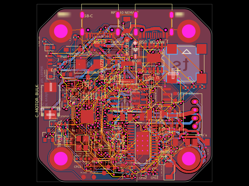 Similar packageimrishabh18/rp2040-motor-controllerA four-layer RP2040-based NEMA17 stepper controller with USB-C power/data, CH224K USB-PD negotiation, DRV8825 dual H-bridge drive, current/temperature telemetry, RGB status LED, buzzer alarm, QSPI flash, and optional AS5600 encoder.
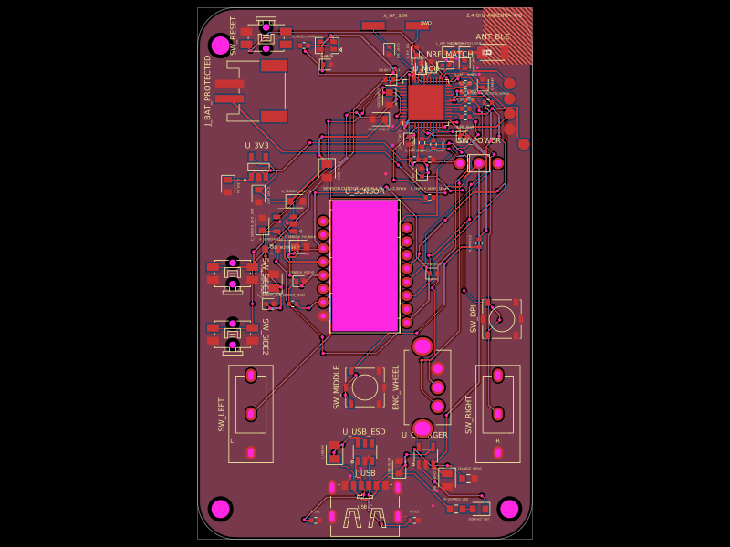 Discover something newMustafaMulla29/wireless-mouse-pcbA hardware component library defining footprints and 3D models for a 3.3 V regulator, RF antenna, switches, connectors, battery charger, and nRF52810 Bluetooth microcontroller.