astra/f1c100s
The code defines the physical pin layout, labels, and footprint for the F1C100S system-on-chip (SoC) component used in electronic devices.
- Version
- 0.9.2
- License
- unset
- Stars
- 0
scripts/optimize-routes.ts
import { checkCapacitorOrientation } from "./check-capacitor-orientation";
import { checkConventionalRouting } from "./check-conventions";
import { readFile, writeFile } from "node:fs/promises";
import { LAYOUT_PROFILES, assertLayoutProfile } from "../src/profiles";
import { validateCircuit, circuitMetrics } from "./validate";
type P = { x: number; y: number; [key: string]: any };
const distance = (a: P, b: P) => Math.hypot(a.x - b.x, a.y - b.y);
function pointSegment(p: P, a: P, b: P) {
	const dx = b.x - a.x,
		dy = b.y - a.y,
		d = dx * dx + dy * dy;
	const t = d
		? Math.max(0, Math.min(1, ((p.x - a.x) * dx + (p.y - a.y) * dy) / d))
		: 0;
	return Math.hypot(p.x - a.x - t * dx, p.y - a.y - t * dy);
}
const cross = (a: P, b: P, c: P) =>
	(b.x - a.x) * (c.y - a.y) - (b.y - a.y) * (c.x - a.x);
function segmentDistance(a: P, b: P, c: P, d: P) {
	if (
		cross(a, b, c) * cross(a, b, d) < 0 &&
		cross(c, d, a) * cross(c, d, b) < 0
	)
		return 0;
	return Math.min(
		pointSegment(a, c, d),
		pointSegment(b, c, d),
		pointSegment(c, a, b),
		pointSegment(d, a, b),
	);
}
function rectangleDistance(a: P, b: P, p: P) {
	const x = p.x - p.width / 2,
		y = p.y - p.height / 2,
		X = p.x + p.width / 2,
		Y = p.y + p.height / 2;
	if ([a, b].some((q) => q.x >= x && q.x <= X && q.y >= y && q.y <= Y))
		return 0;
	const v = [
		{ x, y },
		{ x: X, y },
		{ x: X, y: Y },
		{ x, y: Y },
	];
	return Math.min(
		...v.map((c, i) => segmentDistance(a, b, c, v[(i + 1) % 4]!)),
	);
}
function obstacles(json: any[]) {
	const traces = json.filter((e) => e.type === "pcb_trace");
	const netByPort = new Map(
		json
			.filter((e) => e.type === "source_trace")
			.flatMap((e) =>
				e.connected_source_port_ids.map((p: string) => [p, e.source_trace_id]),
			),
	);
	const ports = new Map(
		json
			.filter((e) => e.type === "pcb_port")
			.map((e) => [e.pcb_port_id, netByPort.get(e.source_port_id)]),
	);
	const pads = json
		.filter((e) => e.type === "pcb_smtpad")
		.map((e) => ({ ...e, net: ports.get(e.pcb_port_id) }));
	const segments: any[] = [],
		vias: any[] = json
			.filter((e) => e.type === "pcb_plated_hole")
			.map((e) => ({
				...e,
				net: ports.get(e.pcb_port_id),
				r: e.outer_diameter / 2,
			}));
	for (const t of traces)
		for (let i = 0; i < t.route.length; i++) {
			const b = t.route[i],
				a = t.route[i - 1];
			if (b.route_type === "via")
				vias.push({ ...b, net: t.source_trace_id, r: 0.225 });
			if (
				a?.route_type === "wire" &&
				b.route_type === "wire" &&
				a.layer === b.layer &&
				distance(a, b) > 1e-7
			)
				segments.push({
					a,
					b,
					layer: a.layer,
					net: t.source_trace_id,
					r: (Math.max(a.width, b.width) || 0.12) / 2,
					minX: Math.min(a.x, b.x),
					maxX: Math.max(a.x, b.x),
					minY: Math.min(a.y, b.y),
					maxY: Math.max(a.y, b.y),
				});
		}
	return (a: P, b: P, net: string) => {
		const gap = 0.10001,
			r = Math.max(a.width || 0.12, b.width || 0.12) / 2;
		const minX = Math.min(a.x, b.x),
			maxX = Math.max(a.x, b.x),
			minY = Math.min(a.y, b.y),
			maxY = Math.max(a.y, b.y);
		for (const p of pads)
			if (p.net !== net && p.layer === a.layer) {
				const margin = gap + r;
				if (
					p.x + p.width / 2 + margin < minX ||
					p.x - p.width / 2 - margin > maxX ||
					p.y + p.height / 2 + margin < minY ||
					p.y - p.height / 2 - margin > maxY
				)
					continue;
				if (rectangleDistance(a, b, p) < margin) return false;
			}
		for (const v of vias)
			if (v.net !== net) {
				const margin = gap + r + v.r;
				if (
					v.x + margin < minX ||
					v.x - margin > maxX ||
					v.y + margin < minY ||
					v.y - margin > maxY
				)
					continue;
				if (pointSegment(v, a, b) < margin) return false;
			}
		for (const s of segments)
			if (s.net !== net && s.layer === a.layer) {
				const margin = gap + r + s.r;
				if (
					s.maxX + margin < minX ||
					s.minX - margin > maxX ||
					s.maxY + margin < minY ||
					s.minY - margin > maxY
				)
					continue;
				if (segmentDistance(a, b, s.a, s.b) < margin) return false;
			}
		return true;
	};
}
function refreshVias(json: any[]) {
	const byKey = new Map<string, any>();
	for (const t of json.filter((e) => e.type === "pcb_trace"))
		for (const p of t.route)
			if (p.route_type === "via") {
				const key = `${p.x.toFixed(6)},${p.y.toFixed(6)}`;
				if (!byKey.has(key))
					byKey.set(key, {
						type: "pcb_via",
						pcb_via_id: `pcb_via_${byKey.size}`,
						pcb_trace_id: t.pcb_trace_id,
						x: p.x,
						y: p.y,
						hole_diameter: 0.2,
						outer_diameter: 0.45,
						layers: ["top", "inner1", "inner2", "bottom"],
						from_layer: p.from_layer,
						to_layer: p.to_layer,
						subcircuit_id: t.subcircuit_id,
					});
			}
	return [...json.filter((e) => e.type !== "pcb_via"), ...byKey.values()];
}
const isConventional = (a: P, b: P) => {
	const dx = Math.abs(b.x - a.x),
		dy = Math.abs(b.y - a.y);
	return Math.min(dx, dy, Math.abs(dx - dy)) < 1e-7;
};
function conventionalPaths(a: P, b: P): P[][] {
	if (isConventional(a, b)) return [[a, b]];
	const dx = b.x - a.x,
		dy = b.y - a.y,
		d = Math.min(Math.abs(dx), Math.abs(dy));
	const point = (x: number, y: number) => ({
		route_type: "wire",
		x,
		y,
		layer: a.layer,
		width: a.width ?? 0.12,
	});
	return [
		[a, point(a.x + Math.sign(dx) * d, a.y + Math.sign(dy) * d), b],
		[a, point(b.x - Math.sign(dx) * d, b.y - Math.sign(dy) * d), b],
		[a, point(a.x, b.y), b],
		[a, point(b.x, a.y), b],
	].map((path) =>
		path.filter((p, i) => !i || distance(p, path[i - 1]!) > 1e-8),
	);
}
function shortcut(
	a: P,
	b: P,
	net: string,
	clear: ReturnType<typeof obstacles>,
) {
	return conventionalPaths(a, b).find((path) =>
		path.every((p, i) => !i || clear(path[i - 1]!, p, net)),
	);
}
const selectedProfile = process.argv[2];
if (selectedProfile) assertLayoutProfile(selectedProfile);
for (const profile of selectedProfile ? [selectedProfile] : LAYOUT_PROFILES) {
	const file = `src/generated/${profile}.circuit.json`;
	let json = JSON.parse(await readFile(file, "utf8"));
	const before = circuitMetrics(json);
	for (const t of json.filter((e: any) => e.type === "pcb_trace"))
		for (let i = 0; i < t.route.length; i++) {
			const p = t.route[i];
			if (p.route_type !== "via") continue;
			const a = t.route
				.slice(0, i)
				.findLast((q: any) => q.route_type === "wire");
			const b = t.route.slice(i + 1).find((q: any) => q.route_type === "wire");
			if (!a || !b) throw Error("Via without contacts");
			p.from_layer = a.layer;
			p.to_layer = b.layer;
		}

	for (let pass = 0; pass < 2; pass++) {
		for (const t of json.filter((e: any) => e.type === "pcb_trace")) {
			const clear = obstacles(json);
			const old = t.route;
			const result: P[] = [];
			for (let i = 0; i < old.length; i++) {
				const a = old[i];
				result.push(a);
				if (a.route_type !== "wire") continue;
				for (let j = old.length - 1; j > i + 1; j--) {
					const b = old[j];
					if (b.route_type !== "wire" || b.layer !== a.layer) continue;
					const path = shortcut(a, b, t.source_trace_id, clear);
					if (path) {
						result.push(...path.slice(1, -1));
						i = j - 1;
						break;
					}
				}
			}
			// Replace a short A→B→C detour with A→C at its existing second via.
			for (let i = 1; i < result.length - 1; i++) {
				const v = result[i],
					a = result[i - 1];
				if (v.route_type !== "via" || a.route_type !== "wire") continue;
				let j = i + 1;
				while (j < result.length && result[j]!.route_type !== "via") j++;
				const w = result[j];
				if (!w || distance(v, w) > 2 || v.from_layer === w.to_layer) continue;
				const incoming = {
					route_type: "wire",
					x: w.x,
					y: w.y,
					layer: v.from_layer,
					width: 0.12,
				};
				const path = shortcut(a, incoming, t.source_trace_id, clear);
				if (path) {
					result.splice(i, j - i + 1, ...path.slice(1), {
						...w,
						from_layer: v.from_layer,
					});
				}
			}
			t.route = result;
		}
		json = refreshVias(json);
	}
	// Exact imported pad centers are not all on the routing grid. Fix their
	// tiny entry/exit offsets as well; never leave an arbitrary-angle segment.
	for (const t of json.filter((e: any) => e.type === "pcb_trace")) {
		const clear = obstacles(json),
			route: P[] = [];
		for (const b of t.route) {
			const a = route.at(-1);
			if (
				a?.route_type === "wire" &&
				b.route_type === "wire" &&
				a.layer === b.layer &&
				!isConventional(a, b)
			) {
				const path = shortcut(a, b, t.source_trace_id, clear);
				if (!path) throw Error(`Cannot make ${t.pcb_trace_id} octilinear`);
				route.push(...path.slice(1));
			} else route.push(b);
		}
		t.route = route;
	}
	const errors = [
		...(await validateCircuit(json)),
		...checkConventionalRouting(json),
		...checkCapacitorOrientation(json),
	];
	if (errors.length) {
		console.log(profile, errors.slice(0, 5));
		throw new Error(`${profile}: ${errors.length} DRC errors`);
	}
	const after = circuitMetrics(json);
	await writeFile(file, JSON.stringify(json, null, 2) + "\n");
	await writeFile(
		`src/generated/${profile}.metrics.json`,
		JSON.stringify(
			{
				...JSON.parse(
					await readFile(`src/generated/${profile}.metrics.json`, "utf8"),
				),
				...after,
				drcErrors: 0,
				optimization: { before, after },
			},
			null,
			2,
		) + "\n",
	);
	console.log(profile, JSON.stringify({ before, after }));
}
Related Packages
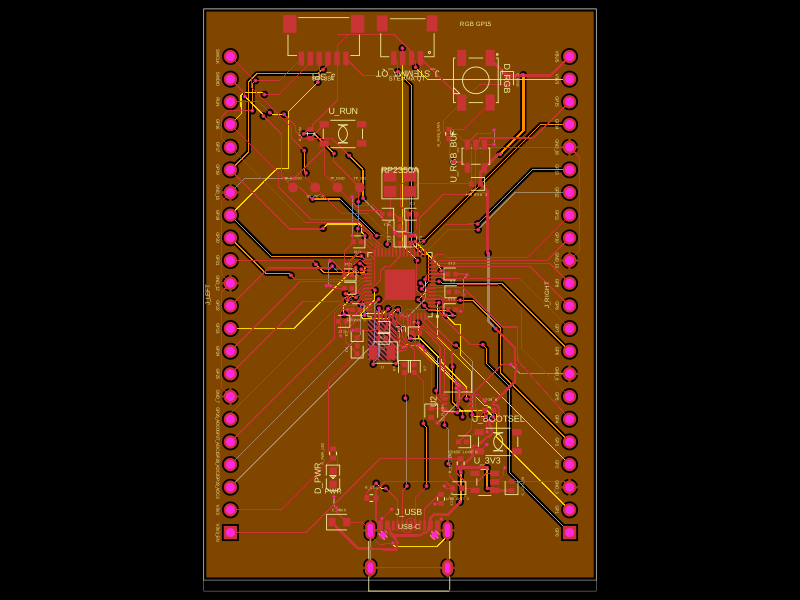 Similar packageabse/rp2350-mcu-boardThis code defines a compact, four-layer PCB hardware layout for the Raspberry Pi RP2350A microcontroller module, including the main IC, power regulation, USB-C connector, STM32-compatible headers, and associated passive components, with detailed component footprints, net connections, and copper pour zones for powering and ground references.
 Discover something newhrithik18k/smart-switch-pcbThe AO3400A component models a SOT-23 N-channel MOSFET with labeled pins for Gate, Source, and Drain, including 3D CAD models and schematic symbols for electronic circuit design.