anil08607/Smartwatch
A 46 mm smartwatch PCB built around an nRF52810 BLE MCU, with USB‑C PD/Li‑ion charging, buck‑boost power, LCD, accelerometer, RTC, buttons, haptic motor, crystals, antenna, and SWD programming connector.
- Version
- 1.0.14
- License
- unset
- Stars
- 0
routing/finalize-native.py
PCB

Schematic

"""Reproduce the reviewed native finishing operations from the saved SES.

Run with KiCad 10's Python: python routing/finalize-native.py build/replayed
This is specific to the committed routing seed. New layouts require a new review.
"""
import sys, math, json, shutil
from pathlib import Path
import pcbnew as p
import wx

wx.Log.SetLogLevel(0)
app = wx.App(False)
out = Path(sys.argv[1] if len(sys.argv) > 1 else 'build/replayed')
out.mkdir(parents=True, exist_ok=True)
source = p.LoadBoard(str(Path('routing/native/placement.kicad_pcb').resolve()))
routed = p.LoadBoard(str(Path('routing/native/router-base.kicad_pcb').resolve()))
assert p.ImportSpecctraSES(routed, str(Path('routing/native/routed.ses').resolve()))
held = []
rf_nets = {"RF_ANT", "RF_50", "RF_FEED"}
fixed_rf = [(t.GetNetname(), p.VECTOR2I(t.GetStart().x,t.GetStart().y), p.VECTOR2I(t.GetEnd().x,t.GetEnd().y), t.GetLayer(), p.ToMM(t.GetWidth())) for t in source.GetTracks() if t.GetNetname() in rf_nets]
for t in list(source.GetTracks()):
    source.Delete(t)

def point(x, y):
    return p.VECTOR2I(p.FromMM(100 + x), p.FromMM(100 - y))

def add_segment(net, start, end, layer, width):
    t = p.PCB_TRACK(source)
    t.SetStart(start)
    t.SetEnd(end)
    t.SetLayer(layer)
    t.SetWidth(p.FromMM(width))
    source.Add(t)
    t.SetNet(source.FindNet(net))
    return t

for t in routed.GetTracks():
    name = t.GetNetname()
    if name in rf_nets:
        continue
    if isinstance(t, p.PCB_VIA):
        item = p.PCB_VIA(source)
        item.SetPosition(t.GetPosition())
        item.SetWidth(t.GetWidth(p.F_Cu))
        item.SetDrill(t.GetDrillValue())
        item.SetViaType(t.GetViaType())
        item.SetLayerPair(t.TopLayer(), t.BottomLayer())
        source.Add(item)
        item.SetNet(source.FindNet(name))
    else:
        layer = t.GetLayer()
        item = add_segment(name, t.GetStart(), t.GetEnd(), layer, max(.1, p.ToMM(t.GetWidth())))
    assert item.GetNetname() == name

for args in fixed_rf:
    add_segment(*args)

# Reviewed explicit finish: preserve the original MCU button escape and RF plane.
finish=json.loads(Path('routing/native/side-access-finishing.json').read_text())
for t in list(source.GetTracks()):
    remove=t.GetNetname() in finish['replace_nets']
    if not isinstance(t,p.PCB_VIA):
        ends={(t.GetStart().x,t.GetStart().y),(t.GetEnd().x,t.GetEnd().y)}
        for expected in finish['remove_tracks']:
            wanted={(point(v['x'],v['y']).x,point(v['x'],v['y']).y) for v in expected['route']}
            if t.GetNetname()==expected['net'] and all(any(abs(a[0]-b[0])<=1000 and abs(a[1]-b[1])<=1000 for b in wanted) for a in ends):remove=True
    if remove:source.Delete(t)
layer_ids={'top':p.F_Cu,'inner1':p.In1_Cu,'inner2':p.In2_Cu,'bottom':p.B_Cu}
for item in finish['tracks']:
    a,b=item['route'];add_segment(item['net'],point(a['x'],a['y']),point(b['x'],b['y']),layer_ids[a['layer']],a['width'])
for item in finish['vias']:
    via=p.PCB_VIA(source);via.SetPosition(point(item['x'],item['y']));via.SetWidth(p.FromMM(item['outer_diameter']));via.SetDrill(p.FromMM(item['hole_diameter']));via.SetViaType(p.VIATYPE_THROUGH);via.SetLayerPair(p.F_Cu,p.B_Cu);source.Add(via);via.SetNet(source.FindNet(item['net']))

for z in list(source.Zones()):
    if not z.GetIsRuleArea():
        source.Delete(z)
        continue
    if z.GetIsRuleArea():
        z.SetDoNotAllowTracks(False)  # RF_FEED is checked separately; pours/vias remain forbidden.
        z.SetDoNotAllowVias(True)
        z.SetDoNotAllowPads(False)
        z.SetDoNotAllowFootprints(False)
for layer in (p.F_Cu, p.In1_Cu, p.In2_Cu, p.B_Cu):
    z = p.ZONE(source)
    z.SetLayer(layer)
    z.SetNet(source.FindNet('GND'))
    z.SetLocalClearance(p.FromMM(.15))
    z.SetThermalReliefGap(p.FromMM(.2))
    z.SetThermalReliefSpokeWidth(p.FromMM(.2))
    z.SetPadConnection(p.ZONE_CONNECTION_FULL)
    z.SetMinThickness(p.FromMM(.1))
    poly = z.Outline()
    poly.NewOutline()
    for cx, cy, angle in [(15, 15, 0), (-15, 15, 90), (-15, -15, 180), (15, -15, 270)]:
        for i in range(17):
            t = math.radians(angle + i * 90 / 16)
            a = point(cx + 7.7 * math.cos(t), cy + 7.7 * math.sin(t))
            poly.Append(a.x, a.y)
    source.Add(z)

pretty = out / 'Smartwatch.pretty'
pretty.mkdir(exist_ok=True)
for f in source.GetFootprints():
    f.Value().SetVisible(False)
    f.Reference().SetVisible(False)
    for item in list(f.GraphicalItems()):
        if item.GetLayer() in (p.F_SilkS, p.B_SilkS):
            held.append(item)
            f.Remove(item)
    f.SetFPID(p.LIB_ID('Smartwatch', f.GetReference() + '_exact'))
    p.PCB_IO_KICAD_SEXPR().FootprintSave(str(pretty.resolve()), f)
for item in list(source.GetDrawings()):
    if item.GetLayer() in (p.F_SilkS, p.B_SilkS):
        source.Delete(item)
text = p.PCB_TEXT(source)
text.SetText('ANIL')
text.SetPosition(point(-20, 11))
text.SetTextSize(p.VECTOR2I(p.FromMM(.8), p.FromMM(.8)))
text.SetTextThickness(p.FromMM(.12))
text.SetLayer(p.F_SilkS)
source.Add(text)
source.GetDesignSettings().SetAuxOrigin(point(-23, -23))
p.ZONE_FILLER(source).Fill(source.Zones())
p.SaveBoard(str((out / 'smartwatch-nrf52810.kicad_pcb').resolve()), source)
shutil.copyfile('routing/native/placement.kicad_pro', out / 'smartwatch-nrf52810.kicad_pro')
print('Replayed side-access copper, preserved critical routes, refilled ground and refreshed silk. Run native checks before accepting.')
Related Packages
 More from this authoranil08607/issue1This code defines a schematic diagram of a DS3231MZ real-time clock (RTC) integrated circuit connected to a 3.3V power supply, I2C data lines, and control signals on a PCB.
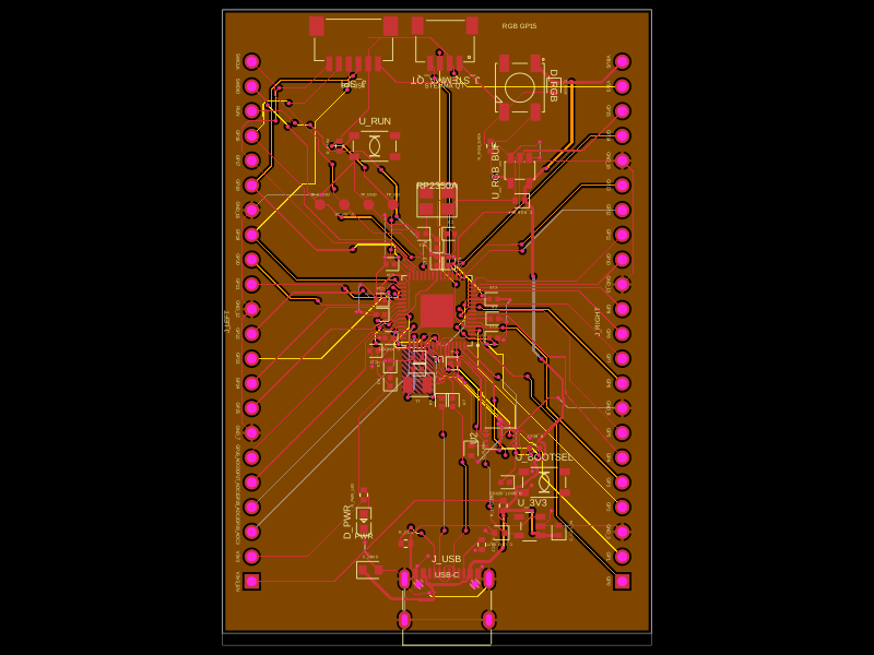 Similar packageabse/rp2350-mcu-boardThis code defines a compact, four-layer PCB hardware layout for the Raspberry Pi RP2350A microcontroller module, including the main IC, power regulation, USB-C connector, STM32-compatible headers, and associated passive components, with detailed component footprints, net connections, and copper pour zones for powering and ground references.
 Discover something newgokul/usb-hub-boardA 4-layer 100×66 mm USB 2.0 hub board with a USB‑C upstream port, four protected downstream USB‑C/USB‑A ports, an integrated SD card reader, USB hub controllers, 3.3 V regulation, ESD protection, current-limited power switches, crystal oscillators, and filtering/passive components.