anil08607/Smartwatch
A 46 mm smartwatch PCB built around an nRF52810 BLE MCU, with USB‑C PD/Li‑ion charging, buck‑boost power, LCD, accelerometer, RTC, buttons, haptic motor, crystals, antenna, and SWD programming connector.
- Version
- 1.0.14
- License
- unset
- Stars
- 0
docs/bring-up.md
# First-article verification

Record instrument, serial number, firmware commit, conditions, measured result and pass/fail for every step. No result below is pre-filled as passed.

1. With all power removed, inspect assembly orientation and hidden joints. Check USB5V, SYS, BAT and V3V0 resistance to GND. Verify J2/J5/J3 harness mappings independently.
2. With battery, LCD and motor disconnected, use a current-limited 5 V source and USB-PD analyzer. Confirm the fixed PD request remains 5 V under every attach/detach sequence. Verify PD_VIN after the 10 Ω/1 µF filter.
3. Measure SYS and the nominal 3.05 V V3V0 rail. Check startup, ripple, load response, short-circuit behavior and temperatures. Confirm the LCD supply remains within 2.5–3.3 V across tolerance, battery and load conditions.
4. Connect a VTref-sensing SWD probe through J3 without backfeeding the board. Identify nRF52810, program/verify, configure reset on P0.21 if required by the Nordic UICR procedure, and test reset. Keep DCDCEN=0. Confirm all three supplies and DEC1–DEC4 nodes against Nordic requirements.
5. Start both Nordic crystal oscillators and the external RTC. Measure startup reliability over temperature and low battery; record frequency accuracy, drift and sleep current. Run BLE radio tests and inspect all four ground layers and the RF feed reference before tuning.
6. Enumerate BMA456 at 0x18, PCF8563 at 0x51 and BQ25180 at 0x6A. Load Bosch's required feature configuration. Test interrupts, motion orientation, RTC alarm and time retention.
7. With power removed, attach the LCD. Initialize SPI conservatively and use line/tile buffers. Keep backlight and motor off initially. Measure backlight current/brightness at the 3.05 V rail before changing its series resistor.
8. Attach only a polarity-verified protected 1S pack with bonded NTC. Begin at 100 mA charge current and 4.2 V termination, subject to the actual pack specification. Verify NTC hot/cold, open and short faults, charge suspend, termination, USB removal, power-path transitions and enclosure temperature.
9. Pulse the motor; measure rail droop, flyback behavior, GPIO default state and unintended resets. Test both buttons and charger/RTC/accelerometer interrupts.
10. Tune RF with the chosen PCB stackup and closed enclosure. Record VNA results, conducted/radiated performance and any matching changes. Test battery runtime, sleep current, ESD, sweat/retention/drop, display-flex durability and charging under load before approving wearable use.

`release/qualification.json` is the release gate record. Attach evidence before changing any pending result to passed.
Related Packages
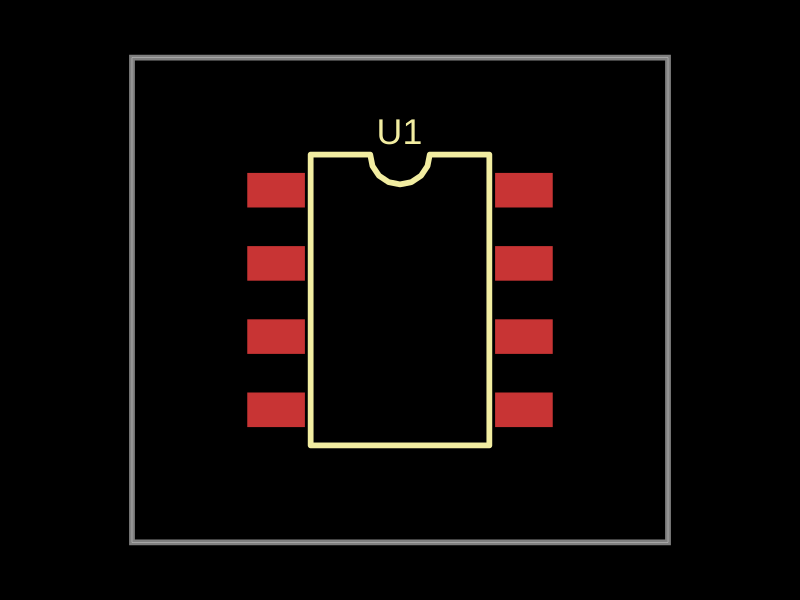 More from this authoranil08607/issue1This code defines a schematic diagram of a DS3231MZ real-time clock (RTC) integrated circuit connected to a 3.3V power supply, I2C data lines, and control signals on a PCB.
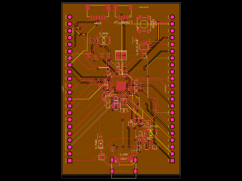 Similar packageabse/rp2350-mcu-boardThis code defines a compact, four-layer PCB hardware layout for the Raspberry Pi RP2350A microcontroller module, including the main IC, power regulation, USB-C connector, STM32-compatible headers, and associated passive components, with detailed component footprints, net connections, and copper pour zones for powering and ground references.
 Discover something newgokul/usb-hub-boardA 4-layer 100×66 mm USB 2.0 hub board with a USB‑C upstream port, four protected downstream USB‑C/USB‑A ports, an integrated SD card reader, USB hub controllers, 3.3 V regulation, ESD protection, current-limited power switches, crystal oscillators, and filtering/passive components.