abse/gameboy-advance
Validates and exports a four-layer Game Boy–style PCB assembly with RP2350 MCU, 32MB flash, USB-C, LCD and speaker connectors, battery buck-boost power, buttons, and verified routing, connectivity, clearances, CAD models, and physical DRC.
- Version
- 0.0.39
- License
- unset
- Stars
- 0
checks/trace-length-review.md
PCB

Schematic

# Reviewed trace bounds

Nine finite, per-trace overrides replace the blanket 5.5 mm bound. Copper geometry, widths, clearances and local capacitor-to-device constraints are unchanged.

| Trace | Limit mm | Basis |
|---|---:|---|
| XIN_IOVDD4_GND_BRIDGE | 8 | Shared ground bridge between capacitors, not crystal load-cap signal connection. |
| V3V3_AVDD_ADC_BRIDGE | 10 | Upstream supply feed. Local ADC bypass positive connection is 1.861 mm. |
| AMP_CAP_GROUND_BRIDGE | 7 | Common ground link between EMI capacitor and amplifier bypass capacitor. |
| VBUS_XOUT_OFFPAD_GROUND | 9 | Ground bridge between unrelated USB and oscillator returns. |
| IOVDD6_IOVDD5_BRIDGE | 8 | Rail distribution. Individual MCU bypass connections are 2.133 and 2.150 mm. |
| QSPI_IOVDD6_GND_BRIDGE | 10 | Both barrels join the same inner1 ground plane. |
| BAT_INPUT_CAP_B | 6.5 | Supplemental bulk capacitor connection is 5.848 mm. Primary 10 uF bypass is 2.405 mm; other bulk connection is 4.844 mm. Both retain 5.5 mm limits. |
| BAT_OUTPUT_FEEDBACK_LINK | 11 | Output-capacitor rail tap to divider top, not high-impedance divider-to-FB node. Horizontal route is 6.782 mm plus checker-counted 3.2 mm for two full-depth transitions. |
| PSRAM_VSS_GND_BRIDGE | 12 | Both barrels join same inner1 plane. Capacitor ground stub is 0.799 mm; positive bypass is 2.350 mm. Bridge total is not the sole bypass return path. |

Ground proof: (2.9,9.55), (5.9,12.2), (9.35,8.55), (13.75,4.09251) lie in the same 10920.42 mm² inner1 ground polygon. Full connectivity/clearance and Gerber shorts checks remain mandatory.

TI TPS63070 datasheet https://www.ti.com/lit/ds/symlink/tps63070.pdf: preserve close primary capacitors, short switching loops, quiet feedback. Bounds are engineering placement limits, not manufacturer-prescribed universal 5.5 mm cutoffs. Electrical performance still requires prototype qualification.

Tenth Errors-tab diagnostic: obsolete schPinSpacing ignored-property warning; removed from U_BAT_BUCKBOOST.

## R8 exterior control move

- SD_BULK: 10 mm supplementary 1 uF supply bound, includes two full-barrel transitions. The primary 100 nF SD bypass is placed with the socket and its positive connection is a short direct top-layer route under the original 5.5 mm bound.
- SD_CMD_PULLUP_V3V3, SD_DAT0_PULLUP_V3V3: 10 mm bounds on resistor pull-up supply feeds, not local capacitor loops.
- USB_CC1_GROUND_BRIDGE: 12 mm common-ground distribution bound after moving USB-C outward.
- The SD 0402 ground fanout uses 0.2 mm copper, above the preserved 0.1 mm net minimum; it joins the inner ground plane through an actual 0.3/0.45 mm via. Main regulator and power-path widths are preserved.
Related Packages
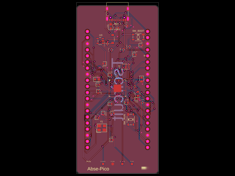 More from this authorabse/abse-picoThis code defines 3D models and footprints for various electronic components—such as voltage regulators, microcontrollers, and memory chips—highlighting their physical pin configurations, mounting pads, and visual identifiers for PCB design.
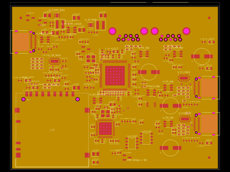 Similar packagegokul/usb3-sd-hubEngineering draft: four-layer, computer-powered USB 3 hub with one USB-C host socket, two USB-C and two USB-A accessory sockets, and a full-size SD slot. Board and three schematic previews are available. Routing and production checks are incomplete; not fabrication ready.
 Discover something newhrithik18k/smart-switch-pcbThe AO3400A component models a SOT-23 N-channel MOSFET with labeled pins for Gate, Source, and Drain, including 3D CAD models and schematic symbols for electronic circuit design.