abse/gameboy-advance
Validates and exports a four-layer Game Boy–style PCB assembly with RP2350 MCU, 32MB flash, USB-C, LCD and speaker connectors, battery buck-boost power, buttons, and verified routing, connectivity, clearances, CAD models, and physical DRC.
- Version
- 0.0.39
- License
- unset
- Stars
- 0
PCB_USER_NOTES.txt
PCB USER / PROTOTYPE BRING-UP NOTES

Battery connector pin 1 = positive, pin 2 = ground. Use four alkaline AA cells.
This board does not charge AA cells. Check holder wiring before connecting.
Begin with a current-limited bench supply and inspect for shorts first.
Confirm the3.234V logic rail and1.1V core supply voltages before connecting the display.
BOOTSEL selects USB boot mode; RUN resets the MCU. Ground/SWDIO/SWCLK/3V3
pads are for a compatible 3.3 V debug probe. Never apply 5 V to logic pins.
Speaker connector pin 1 = amplifier output plus; pin 2 = output minus.
Both speaker wires are driven: do not connect either to chassis/ground.
Use the specified8-ohm1W speaker. R_SPK_LIMIT provides passive attenuation;
check actual output, pops and maximum volume on the bench.
Insert the specified LCD flex with its contacts facing the connector contacts;
open its latch first. Disconnect power before inserting/removing the flex.
Check every button released and pressed before installing the enclosure.
A released switch must not short its GPIO to ground; pressing it must do so.
Firmware and USB/display qualification remain necessary before product use.

Pass the assembled JST PHR-2 battery plug through the rectangular PCB
opening before mating it to J_BAT. Protect leads from the milled edge and
provide cable slack/strain relief; do not force the plug through an old PCB.

Legacy V3V3/TP_3V3 names now denote the nominal3.234V logic rail.
See ELECTRICAL_PROTOTYPE_REVIEW.txt for the prototype load/ripple allowances.
Related Packages
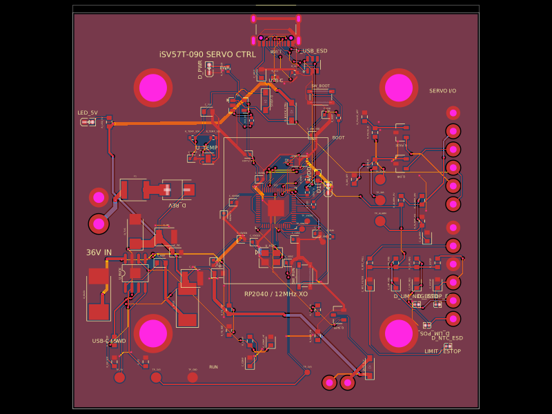 More from this authorabse/isv57t090-motion-controllerA 36 V-powered RP2040 motion-controller PCB that regulates 5 V, drives isolated STEP/DIR servo inputs, monitors alarms, temperature, limits and E-stop signals, and provides protected safety/field connectors.
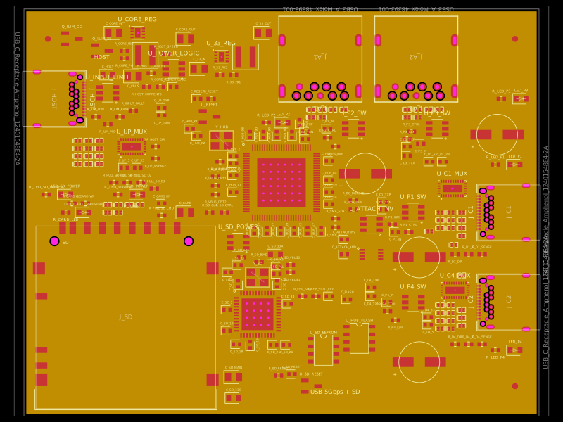 Similar packagegokul/usb3-sd-hubEngineering draft: four-layer, computer-powered USB 3 hub with one USB-C host socket, two USB-C and two USB-A accessory sockets, and a full-size SD slot. Board and three schematic previews are available. Routing and production checks are incomplete; not fabrication ready.
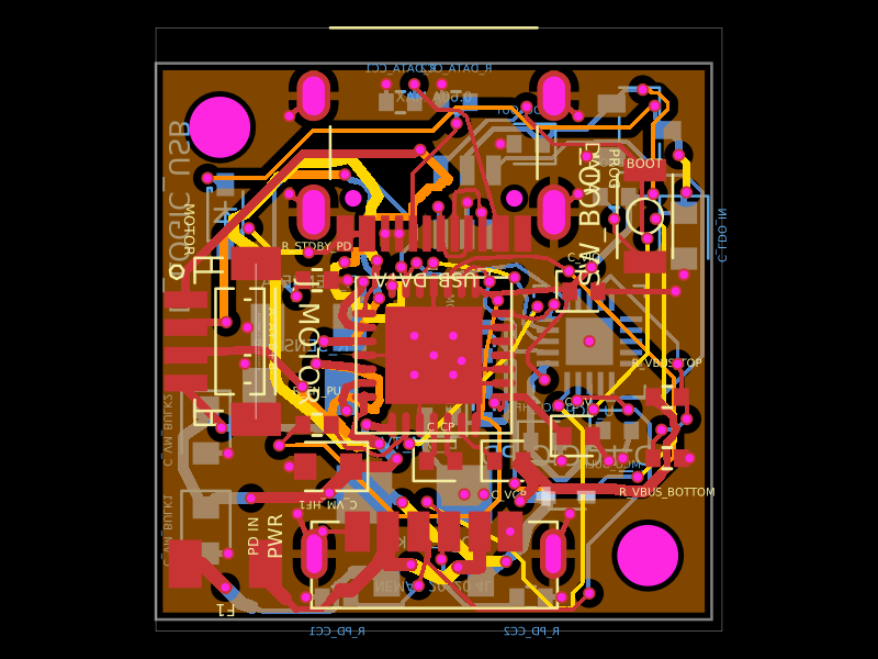 Discover something newShiboSoftwareDev/nema8-20mm-usbc-pd-controllerA 20×20 mm four-layer USB‑C PD stepper motor controller PCB using a CH32X035 MCU, TMC2209 driver, protected power inputs, USB data/boot interface, 3.3 V regulation, ESD/TVS protection, current-sense circuitry, and NEMA‑8 motor outputs.