abse/gameboy-advance
Validates and exports a four-layer Game Boy–style PCB assembly with RP2350 MCU, 32MB flash, USB-C, LCD and speaker connectors, battery buck-boost power, buttons, and verified routing, connectivity, clearances, CAD models, and physical DRC.
- Version
- 0.0.39
- License
- unset
- Stars
- 0
CONNECTOR_ACCESS_REVIEW.txt
CONNECTOR ACCESS REVIEW / BATTERY FEED-THROUGH REVISION

JST PHR-2 manufacturer housing:5.8 mm width,4.5 mm depth,6.85 mm length.
The previous 6 mm round PCB hole did not contain its 5.8 x4.5 mm cross-section.
New non-plated PCB opening:8 x8 mm at(15,-35), with up to0.5 mm milled
corner radius. Feeding along the plug length leaves1.1 mm lateral and1.75 mm depth
clearance per side. Feeding it already oriented for the horizontal header
uses a5.8 x6.85 mm projection, with1.1 mm and0.575 mm clearance per side. CAD plug dimensions are a drawing-based clearance envelope,
not a replacement supplier component model.

Other access scenarios reviewed against existing R13 geometry and sequence:
- Holder-cradle exit is a lateral opening:the cut is5 mm long in X,
 9 mm in Y and8 mm in Z. Plug travel is along X, so the limiting passage
 is9 x8 mm, not5 x9 mm. The PH plug fits with its5.8 x4.5 mm cross-section.
- Speaker SH plug is installed from the open front during assembly; it does
 not pass through the battery opening or a closed shell wall.
- USB opening is15 mm wide x7 mm high. The plug metal enters before the
 overmould reaches the shell; check the actual intended cable during fit-print.
 There is no universal overmould size guarantee.
- microSD exterior opening is19 mm wide x5 mm high; the card is11 mm wide
 and1 mm thick. Retain the established outward insertion/ejection path.
- LCD flex is inserted with latch access before the display retainer is closed.
 Retain the top-contact connector and verified flat reinforced flex tip.
- Battery holder remains mounted to rear-shell inserts, independently of PCB.
 No screw positions, button caps, shell latches or grip dimensions change.

PCB ground branch formerly crossed a corner of the enlarged opening. Its
local detour preserves the0.8 mm width and restores the original path beyond
the opening. The new build checks all traces, vias and pads for at least0.3 mm
cutout clearance, alongside the existing net, DRC and contact audits.
Physical fit-print, insertion force and cable strain relief remain bench checks.

Copper-pour clearance remains0.25 mm, exceeding JLCPCB's0.2 mm routed-slot
minimum. The new build audit's0.4 mm minimum applies to traces, pads and vias.
Reference:https://jlcpcb.com/capabilities/pcb-capabilities (Patterns Routed).
Related Packages
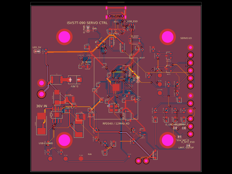 More from this authorabse/isv57t090-motion-controllerA 36 V-powered RP2040 motion-controller PCB that regulates 5 V, drives isolated STEP/DIR servo inputs, monitors alarms, temperature, limits and E-stop signals, and provides protected safety/field connectors.
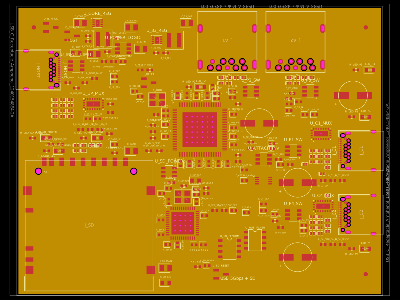 Similar packagegokul/usb3-sd-hubEngineering draft: four-layer, computer-powered USB 3 hub with one USB-C host socket, two USB-C and two USB-A accessory sockets, and a full-size SD slot. Board and three schematic previews are available. Routing and production checks are incomplete; not fabrication ready.
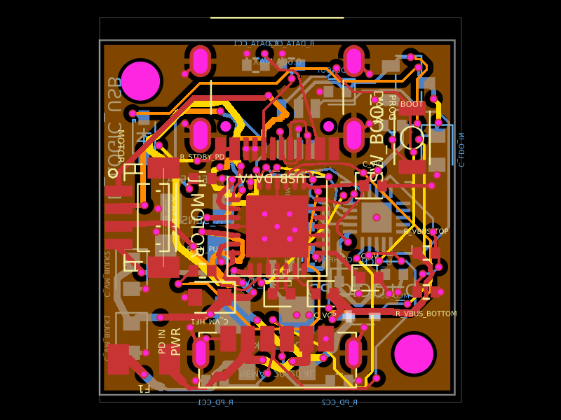 Discover something newShiboSoftwareDev/nema8-20mm-usbc-pd-controllerA 20×20 mm four-layer USB‑C PD stepper motor controller PCB using a CH32X035 MCU, TMC2209 driver, protected power inputs, USB data/boot interface, 3.3 V regulation, ESD/TVS protection, current-sense circuitry, and NEMA‑8 motor outputs.