abse/boostxl-sharp128
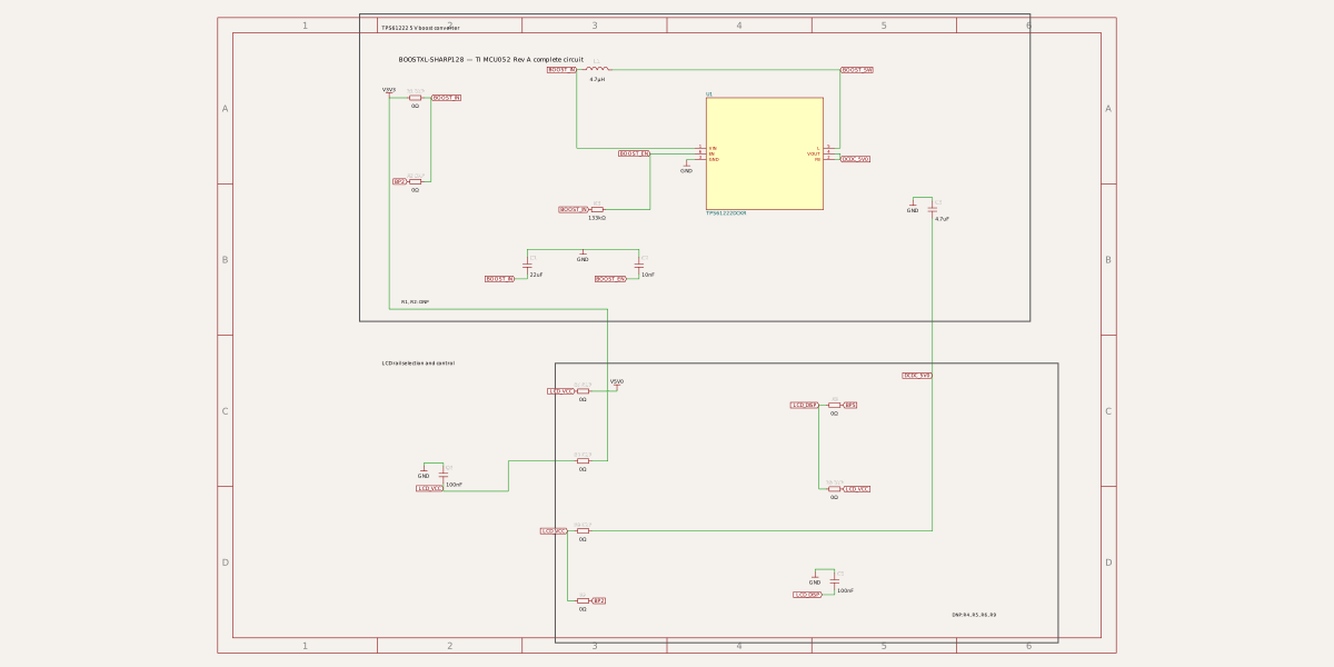
This code defines a printed circuit board (PCB) with various surface-mount resistors, capacitors, inductors, and integrated circuits, including power management components and interface connectors, for a TI-based LCD and microSD module using 0603 and other package types.
- Version
- 1.0.0
- License
- unset
- Stars
- 0
index.circuit.tsx
PCB
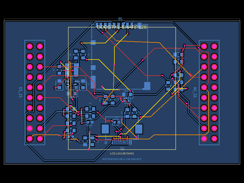
Schematic
import { DM3BT_DSF_PEJS } from "./imports/DM3BT_DSF_PEJS"
import { FH12_10S_0_5SH_55_ } from "./imports/FH12_10S_0_5SH_55_"
import { SSQ_110_03_T_D } from "./imports/SSQ_110_03_T_D"
import { TPS61222DCKR } from "./imports/TPS61222DCKR"

const POWER_SHEET = "Power Conversion and LCD Rail Selection"
const LAUNCHPAD_SHEET = "LaunchPad XL Interface"
const LCD_SHEET = "Sharp Memory LCD Interface"
const MICROSD_SHEET = "microSD Interface and Detection"
const SECTION = "TI_MCU052_REV_A_COMPLETE_CIRCUIT"

const N = {
  GND: "net.GND",
  V3V3: "net.V3V3",
  V5V0: "net.V5V0",
  DCDC_5V0: "net.DCDC_5V0",
  BOOST_IN: "net.BOOST_IN",
  BOOST_SW: "net.BOOST_SW",
  BOOST_EN: "net.BOOST_EN",
  LCD_VCC: "net.LCD_VCC",
  LCD_DISP: "net.LCD_DISP",
  LCD_SPI_CS: "net.LCD_SPI_CS",
  LCD_EXTCOMIN: "net.LCD_EXTCOMIN",
  EXT_MODE: "net.EXT_MODE",
  SD_SPI_CS: "net.SD_SPI_CS",
  SD_DETECT: "net.SD_DETECT",
  BP2: "net.BP2",
  BP3: "net.BP3",
  BP4: "net.BP4",
  BP5: "net.BP5",
  BP6: "net.BP6",
  BP7: "net.BP7",
  BP8: "net.BP8",
  BP9: "net.BP9",
  BP10: "net.BP10",
  BP11: "net.BP11",
  BP12: "net.BP12",
  BP13: "net.BP13",
  BP14: "net.BP14",
  BP15: "net.BP15",
  BP16: "net.BP16",
  BP17: "net.BP17",
  BP18: "net.BP18",
  BP19: "net.BP19",
  BP23: "net.BP23",
  BP24: "net.BP24",
  BP25: "net.BP25",
  BP26: "net.BP26",
  BP27: "net.BP27",
  BP28: "net.BP28",
  BP29: "net.BP29",
  BP30: "net.BP30",
  BP31: "net.BP31",
  BP32: "net.BP32",
  BP33: "net.BP33",
  BP34: "net.BP34",
  BP35: "net.BP35",
  BP36: "net.BP36",
  BP37: "net.BP37",
  BP38: "net.BP38",
  BP39: "net.BP39",
  BP40: "net.BP40",
} as const

const ZERO_OHM_MPN = "CRCW06030000Z0EA"

export default () => (
  <board
    name="BOOSTXL_SHARP128"
    title="BOOSTXL-SHARP128"
    width="58.42mm"
    height="35.56mm"
    outline={[
      { x: -29.21, y: -17.78 },
      { x: 29.21, y: -17.78 },
      { x: 29.21, y: 17.78 },
      { x: -29.21, y: 17.78 },
    ]}
    material="fr4"
    layers={4}
    thickness="1.6mm"
    solderMaskColor="red"
    silkscreenColor="white"
    doubleSidedAssembly
    defaultTraceWidth="0.1524mm"
    minViaHoleDiameter="0.3mm"
    minViaPadDiameter="0.45mm"
    schMaxTraceDistance="0mm"
    schTraceAutoLabelEnabled
    placementDrcChecksDisabled
    autorouter={{ preset: "auto_local", local: true, traceClearance: "0.1524mm" }}
    autorouterEffortLevel="5x"
  >
    <schematicsheet name={POWER_SHEET} displayName={POWER_SHEET} sheetIndex={1} />
    <schematicsheet name={LAUNCHPAD_SHEET} displayName={LAUNCHPAD_SHEET} sheetIndex={2} />
    <schematicsheet name={LCD_SHEET} displayName={LCD_SHEET} sheetIndex={3} />
    <schematicsheet name={MICROSD_SHEET} displayName={MICROSD_SHEET} sheetIndex={4} />

    <group
      name="TI_REFERENCE_SCHEMATIC"
      schSheetName={POWER_SHEET}
      schX={0}
      schY={0}
      pcbX={0}
      pcbY={0}
      schMaxTraceDistance="0mm"
      schTraceAutoLabelEnabled
    >
      <schematicsection
        name={SECTION}
        displayName="BOOSTXL-SHARP128 — TI MCU052 Rev A complete circuit"
        sectionTitleFontSize="0.22mm"
      />

    </group>

    <group name="BOOST_CONVERTER" schSheetName={POWER_SHEET} schX={23} schY={-5} pcbX={0} pcbY={0} schMaxTraceDistance="0mm" schTraceAutoLabelEnabled>
      <schematicrect schX={-22} schY={11} width="24mm" height="11mm" strokeWidth="0.04mm" color="#555555" />
      <schematictext text="TPS61222 5 V boost converter" schX={-33.2} schY={16} fontSize={0.18} anchor="left" />
      <resistor name="R1" displayName="R1 DNP" resistance="0ohm" footprint="0603" manufacturerPartNumber={ZERO_OHM_MPN} schSectionName={SECTION} schX={-32} schY={13.5} pcbX={-9.652} pcbY={9.398} pcbRotation={270} layer="bottom" connections={{ pin1: N.V3V3, pin2: N.BOOST_IN }} />
      <resistor name="R2" displayName="R2 DNP" resistance="0ohm" footprint="0603" manufacturerPartNumber={ZERO_OHM_MPN} schSectionName={SECTION} schX={-32} schY={10.5} pcbX={-11.43} pcbY={9.398} pcbRotation={270} layer="bottom" connections={{ pin1: N.BP2, pin2: N.BOOST_IN }} />
      <capacitor name="C1" capacitance="22uF" footprint="0603" manufacturerPartNumber="GRM188R61A226ME15D" schSectionName={SECTION} schX={-28} schY={7.5} schRotation={90} pcbX={-9.652} pcbY={2.04} pcbRotation={270} layer="bottom" connections={{ pin1: N.BOOST_IN, pin2: N.GND }} />
      <inductor
        name="L1"
        inductance="4.7uH"
        manufacturerPartNumber="EPL3015-472MLB"
        schSectionName={SECTION}
        schX={-25.5}
        schY={14.5}
        pcbX={-12.446}
        pcbY={5.596}
        pcbRotation={180}
        layer="bottom"
        footprint={
          <footprint>
            <smtpad portHints={["pin1"]} pcbX="1.04mm" pcbY="0mm" width="1.12mm" height="3.2mm" shape="rect" />
            <smtpad portHints={["pin2"]} pcbX="-1.04mm" pcbY="0mm" width="1.12mm" height="3.2mm" shape="rect" />
            <silkscreenrect pcbX="0mm" pcbY="0mm" width="3.2mm" height="3.2mm" />
          </footprint>
        }
        connections={{ pin1: N.BOOST_IN, pin2: N.BOOST_SW }}
      />
      <TPS61222DCKR
        name="U1"
        schSectionName={SECTION}
        schX={-19.5}
        schY={11.5}
        schWidth="4.2mm"
        schHeight="4mm"
        schPinArrangement={{ leftSide: [1, 6, 3], rightSide: [5, 4, 2] }}
        pcbX={-12.446}
        pcbY={2.04}
        pcbRotation={180}
        layer="bottom"
        connections={{ VIN: N.BOOST_IN, FB: N.DCDC_5V0, GND: N.GND, VOUT: N.DCDC_5V0, L: N.BOOST_SW, EN: N.BOOST_EN }}
      />
      <resistor name="R3" resistance="133k" footprint="0603" manufacturerPartNumber="CRCW0603133KFKEA" schSectionName={SECTION} schX={-25.5} schY={9.5} pcbX={-15.494} pcbY={5.596} pcbRotation={270} layer="bottom" connections={{ pin1: N.BOOST_IN, pin2: N.BOOST_EN }} />
      <capacitor name="C2" capacitance="10nF" footprint="0603" manufacturerPartNumber="GRM188R71E103KA01D" schSectionName={SECTION} schX={-24} schY={7.5} schRotation={90} pcbX={-15.494} pcbY={2.04} pcbRotation={270} layer="bottom" connections={{ pin1: N.BOOST_EN, pin2: N.GND }} />
      <capacitor name="C3" capacitance="4.7uF" footprint="0603" manufacturerPartNumber="GRM188C71A475KE11D" schSectionName={SECTION} schX={-13.5} schY={9.5} schRotation={90} pcbX={-12.446} pcbY={-0.246} pcbRotation={0} layer="bottom" connections={{ pin1: N.DCDC_5V0, pin2: N.GND }} />
      <schematictext text="R1, R2: DNP" schX={-32.5} schY={6.2} fontSize={0.16} anchor="left" />
    </group>

    <group name="LCD_POWER_SELECTION" schSheetName={POWER_SHEET} schX={-3} schY={-17} pcbX={0} pcbY={0} schMaxTraceDistance="0mm" schTraceAutoLabelEnabled>
      <schematicrect schX={8} schY={11} width="18mm" height="10mm" strokeWidth="0.04mm" color="#555555" />
      <schematictext text="LCD rail selection and control" schX={-7.2} schY={16} fontSize={0.18} anchor="left" />
      <capacitor name="C4" capacitance="100nF" footprint="0402" manufacturerPartNumber="GRM155R71A104KA01D" schSectionName={SECTION} schX={-5} schY={12} schRotation={90} pcbX={-12.7} pcbY={-10.922} pcbRotation={180} layer="bottom" connections={{ pin1: N.LCD_VCC, pin2: N.GND }} />
      <resistor name="R4" displayName="R4 DNP" resistance="0ohm" footprint="0603" manufacturerPartNumber={ZERO_OHM_MPN} schSectionName={SECTION} schX={0} schY={15} pcbX={-12.7} pcbY={-9.396} pcbRotation={180} layer="bottom" connections={{ pin1: N.LCD_VCC, pin2: N.V5V0 }} />
      <resistor name="R5" displayName="R5 DNP" resistance="0ohm" footprint="0603" manufacturerPartNumber={ZERO_OHM_MPN} schSectionName={SECTION} schX={0} schY={12.5} pcbX={-12.7} pcbY={-7.62} pcbRotation={180} layer="bottom" connections={{ pin1: N.LCD_VCC, pin2: N.V3V3 }} />
      <resistor name="R6" displayName="R6 DNP" resistance="0ohm" footprint="0603" manufacturerPartNumber={ZERO_OHM_MPN} schSectionName={SECTION} schX={0} schY={10} pcbX={-12.7} pcbY={-5.842} pcbRotation={180} layer="bottom" connections={{ pin1: N.LCD_VCC, pin2: N.DCDC_5V0 }} />
      <resistor name="R7" resistance="0ohm" footprint="0603" manufacturerPartNumber={ZERO_OHM_MPN} schSectionName={SECTION} schX={0} schY={7.5} pcbX={-12.7} pcbY={-4.064} pcbRotation={180} layer="bottom" connections={{ pin1: N.LCD_VCC, pin2: N.BP2 }} />

      <resistor name="R8" resistance="0ohm" footprint="0603" manufacturerPartNumber={ZERO_OHM_MPN} schSectionName={SECTION} schX={9} schY={14.5} pcbX={-7.874} pcbY={-5.842} pcbRotation={180} layer="bottom" connections={{ pin1: N.LCD_DISP, pin2: N.BP5 }} />
      <resistor name="R9" displayName="R9 DNP" resistance="0ohm" footprint="0603" manufacturerPartNumber={ZERO_OHM_MPN} schSectionName={SECTION} schX={9} schY={11.5} pcbX={-7.874} pcbY={-4.064} pcbRotation={180} layer="bottom" connections={{ pin1: N.LCD_DISP, pin2: N.LCD_VCC }} />
      <capacitor name="C5" capacitance="100nF" footprint="0402" manufacturerPartNumber="GRM155R71A104KA01D" schSectionName={SECTION} schX={9} schY={8.2} schRotation={90} pcbX={-7.874} pcbY={-7.366} pcbRotation={180} layer="bottom" connections={{ pin1: N.LCD_DISP, pin2: N.GND }} />
      <schematictext text="DNP: R4, R5, R6, R9" schX={14} schY={7} fontSize={0.16} anchor="center" />
    </group>

    <group name="BOOSTERPACK_INTERFACE" schSheetName={LAUNCHPAD_SHEET} schX={0} schY={0} pcbX={0} pcbY={0} schMaxTraceDistance="0mm" schTraceAutoLabelEnabled>
      <schematicrect schX={0} schY={1.5} width="27mm" height="8mm" strokeWidth="0.04mm" color="#555555" />
      <schematictext text="LaunchPad XL 40-pin BoosterPack interface" schX={-12.8} schY={4.9} fontSize={0.18} anchor="left" />
      <SSQ_110_03_T_D
        name="J1_J3"
        displayName="J1 / J3"
        schSectionName={SECTION}
        schX={-6}
        schY={1.3}
        schWidth="4.5mm"
        schHeight="4mm"
        schPinArrangement={{ leftSide: [1, 3, 5, 7, 9, 11, 13, 15, 17, 19], rightSide: [2, 4, 6, 8, 10, 12, 14, 16, 18, 20] }}
        pcbX={-21.59}
        pcbY={0}
        pcbRotation={90}
        layer="bottom"
        connections={{ pin1: N.V3V3, pin2: N.V5V0, pin3: N.BP2, pin4: N.GND, pin5: N.BP3, pin6: N.BP23, pin7: N.BP4, pin8: N.BP24, pin9: N.BP5, pin10: N.BP25, pin11: N.BP6, pin12: N.BP26, pin13: N.BP7, pin14: N.BP27, pin15: N.BP8, pin16: N.BP28, pin17: N.BP9, pin18: N.BP29, pin19: N.BP10, pin20: N.BP30 }}
      />
      <SSQ_110_03_T_D
        name="J2_J4"
        displayName="J2 / J4"
        schSectionName={SECTION}
        schX={6}
        schY={1.3}
        schWidth="4.5mm"
        schHeight="4mm"
        schPinArrangement={{ leftSide: [1, 3, 5, 7, 9, 11, 13, 15, 17, 19], rightSide: [2, 4, 6, 8, 10, 12, 14, 16, 18, 20] }}
        pcbX={21.59}
        pcbY={0}
        pcbRotation={90}
        layer="bottom"
        connections={{ pin1: N.BP40, pin2: N.GND, pin3: N.BP39, pin4: N.BP19, pin5: N.BP38, pin6: N.BP18, pin7: N.BP37, pin8: N.BP17, pin9: N.BP36, pin10: N.BP16, pin11: N.BP35, pin12: N.BP15, pin13: N.BP34, pin14: N.BP14, pin15: N.BP33, pin16: N.BP13, pin17: N.BP32, pin18: N.BP12, pin19: N.BP31, pin20: N.BP11 }}
      />
    </group>

    <group name="MEMORY_LCD_INTERFACE" schSheetName={LCD_SHEET} schX={18} schY={12} pcbX={0} pcbY={0} schMaxTraceDistance="0mm" schTraceAutoLabelEnabled>
      <schematicrect schX={-18} schY={-11} width="32mm" height="14mm" strokeWidth="0.04mm" color="#555555" />
      <schematictext text="Sharp LS013B7DH03 Memory LCD interface" schX={-33.2} schY={-4.5} fontSize={0.18} anchor="left" />
      <FH12_10S_0_5SH_55_
        name="J5"
        displayName="J5 LCD FPC"
        schSectionName={SECTION}
        schX={-18}
        schY={-10}
        schWidth="5mm"
        schHeight="6mm"
        schPinArrangement={{ leftSide: [1, 2, 3, 4, 5], rightSide: [6, 7, 8, 9, 10], bottomSide: [11, 12] }}
        pcbX={0}
        pcbY={-10.414}
        pcbRotation={180}
        layer="bottom"
        connections={{ pin1: N.BP7, pin2: N.BP15, pin3: N.LCD_SPI_CS, pin4: N.LCD_EXTCOMIN, pin5: N.LCD_DISP, pin6: N.LCD_VCC, pin7: N.LCD_VCC, pin8: N.EXT_MODE, pin9: N.GND, pin10: N.GND }}
        noConnect={["pin11", "pin12"]}
      />
      <capacitor name="C6" capacitance="100nF" footprint="0402" manufacturerPartNumber="GRM155R71A104KA01D" schSectionName={SECTION} schX={-28} schY={-8} schRotation={90} pcbX={-1.27} pcbY={-7.366} pcbRotation={180} layer="bottom" connections={{ pin1: N.LCD_VCC, pin2: N.GND }} />
      <resistor name="R10" displayName="R10 DNP" resistance="4.7k" footprint="0603" manufacturerPartNumber="CRCW06034K70JNEA" schSectionName={SECTION} schX={-27} schY={-12} pcbX={-7.366} pcbY={-12.065} pcbRotation={90} layer="bottom" connections={{ pin1: N.EXT_MODE, pin2: N.LCD_VCC }} />
      <resistor name="R11" resistance="0ohm" footprint="0603" manufacturerPartNumber={ZERO_OHM_MPN} schSectionName={SECTION} schX={-27} schY={-15} pcbX={-9.144} pcbY={-12.065} pcbRotation={270} layer="bottom" connections={{ pin1: N.GND, pin2: N.EXT_MODE }} />
      <resistor name="R12" resistance="0ohm" footprint="0603" manufacturerPartNumber={ZERO_OHM_MPN} schSectionName={SECTION} schX={-12} schY={-14} pcbX={13.97} pcbY={9.398} pcbRotation={0} layer="bottom" connections={{ pin1: N.LCD_EXTCOMIN, pin2: N.GND }} />
      <resistor name="R13" displayName="R13 DNP" resistance="0ohm" footprint="0603" manufacturerPartNumber={ZERO_OHM_MPN} schSectionName={SECTION} schX={-7} schY={-14} pcbX={13.97} pcbY={7.62} pcbRotation={0} layer="bottom" connections={{ pin1: N.LCD_EXTCOMIN, pin2: N.BP19 }} />
      <resistor name="R14" resistance="0ohm" footprint="0603" manufacturerPartNumber={ZERO_OHM_MPN} schSectionName={SECTION} schX={-12} schY={-7} pcbX={1.3035} pcbY={-5.08} pcbRotation={90} layer="bottom" connections={{ pin1: N.LCD_SPI_CS, pin2: N.BP6 }} />
      <resistor name="R15" displayName="R15 DNP" resistance="0ohm" footprint="0603" manufacturerPartNumber={ZERO_OHM_MPN} schSectionName={SECTION} schX={-7} schY={-7} pcbX={3.0815} pcbY={-5.08} pcbRotation={90} layer="bottom" connections={{ pin1: N.LCD_SPI_CS, pin2: N.BP13 }} />
      <schematictext text="DNP: R10, R13, R15" schX={-18} schY={-16.6} fontSize={0.16} anchor="center" />
    </group>

    <group name="MICROSD_INTERFACE" schSheetName={MICROSD_SHEET} schX={-18} schY={12} pcbX={0} pcbY={0} schMaxTraceDistance="0mm" schTraceAutoLabelEnabled>
      <schematicrect schX={18} schY={-11} width="32mm" height="14mm" strokeWidth="0.04mm" color="#555555" />
      <schematictext text="Hirose DM3BT microSD interface" schX={2.8} schY={-4.5} fontSize={0.18} anchor="left" />
      <DM3BT_DSF_PEJS
        name="J6"
        displayName="J6 microSD"
        schSectionName={SECTION}
        schX={18}
        schY={-9.5}
        schWidth="6mm"
        schHeight="6mm"
        schPinArrangement={{ leftSide: [1, 11, 13, 14, 7, 12, 5], rightSide: [2, 3, 4, 6, 8, 9, 10] }}
        pcbX={-0.375}
        pcbY={8.955}
        pcbRotation={0}
        layer="bottom"
        connections={{ pin1: N.GND, pin3: N.SD_SPI_CS, pin4: N.BP15, pin5: N.V3V3, pin6: N.BP7, pin7: N.GND, pin8: N.BP14, pin10: N.SD_DETECT, pin11: N.GND, pin12: N.GND, pin13: N.GND, pin14: N.GND }}
        noConnect={["pin2", "pin9"]}
      />
      <capacitor name="C7" capacitance="1uF" footprint="0603" manufacturerPartNumber="GRM188R71C105KA12D" schSectionName={SECTION} schX={7} schY={-7} schRotation={90} pcbX={1.27} pcbY={-0.508} pcbRotation={0} layer="bottom" connections={{ pin1: N.V3V3, pin2: N.GND }} />
      <capacitor name="C8" capacitance="100nF" footprint="0402" manufacturerPartNumber="GRM155R71A104KA01D" schSectionName={SECTION} schX={10} schY={-7} schRotation={90} pcbX={1.143} pcbY={-2.032} pcbRotation={0} layer="bottom" connections={{ pin1: N.V3V3, pin2: N.GND }} />
      <resistor name="R16" resistance="0ohm" footprint="0603" manufacturerPartNumber={ZERO_OHM_MPN} schSectionName={SECTION} schX={7} schY={-12} pcbX={-4.064} pcbY={-1.778} pcbRotation={270} layer="bottom" connections={{ pin1: N.SD_SPI_CS, pin2: N.BP8 }} />
      <resistor name="R17" displayName="R17 DNP" resistance="0ohm" footprint="0603" manufacturerPartNumber={ZERO_OHM_MPN} schSectionName={SECTION} schX={12} schY={-12} pcbX={-2.286} pcbY={-1.778} pcbRotation={270} layer="bottom" connections={{ pin1: N.SD_SPI_CS, pin2: N.BP12 }} />
      <resistor name="R18" resistance="0ohm" footprint="0603" manufacturerPartNumber={ZERO_OHM_MPN} schSectionName={SECTION} schX={23} schY={-14.5} pcbX={13.97} pcbY={4.318} pcbRotation={0} layer="bottom" connections={{ pin1: N.SD_DETECT, pin2: N.BP17 }} />
      <resistor name="R19" displayName="R19 DNP" resistance="0ohm" footprint="0603" manufacturerPartNumber={ZERO_OHM_MPN} schSectionName={SECTION} schX={29} schY={-10} pcbX={13.97} pcbY={2.54} pcbRotation={0} layer="bottom" connections={{ pin1: N.SD_DETECT, pin2: N.BP18 }} />
      <resistor name="R20" displayName="R20 DNP" resistance="0ohm" footprint="0603" manufacturerPartNumber={ZERO_OHM_MPN} schSectionName={SECTION} schX={29} schY={-13} pcbX={13.97} pcbY={0.762} pcbRotation={0} layer="bottom" connections={{ pin1: N.SD_DETECT, pin2: N.BP11 }} />
      <resistor name="R21" displayName="R21 DNP" resistance="100k" footprint="0603" manufacturerPartNumber="CRCW0603100KFKEA" schSectionName={SECTION} schX={26} schY={-7} schRotation={90} pcbX={11.43} pcbY={1.651} pcbRotation={270} layer="bottom" connections={{ pin1: N.SD_DETECT, pin2: N.V3V3 }} />
      <schematictext text="DNP: R17, R19, R20, R21" schX={22} schY={-16.6} fontSize={0.16} anchor="center" />
    </group>

    <silkscreenrect pcbX="0mm" pcbY="1.016mm" width="26.6mm" height="30.3mm" layer="top" />
    <silkscreentext text="BOOSTXL-SHARP128" pcbX="0mm" pcbY="16.2mm" fontSize="1.2mm" anchorAlignment="center" layer="top" />
    <silkscreentext text="LCD LS013B7DH03" pcbX="0mm" pcbY="-15.1mm" fontSize="0.65mm" anchorAlignment="center" layer="top" />
    <silkscreentext text="TI MCU052 REV A RECONSTRUCTION" pcbX="0mm" pcbY="-16.5mm" fontSize="0.55mm" anchorAlignment="center" layer="bottom" />

    <copperpour name="GND_BOTTOM_POUR" layer="bottom" connectsTo={N.GND} clearance="0.18mm" boardEdgeMargin="0.25mm" />
  </board>
)