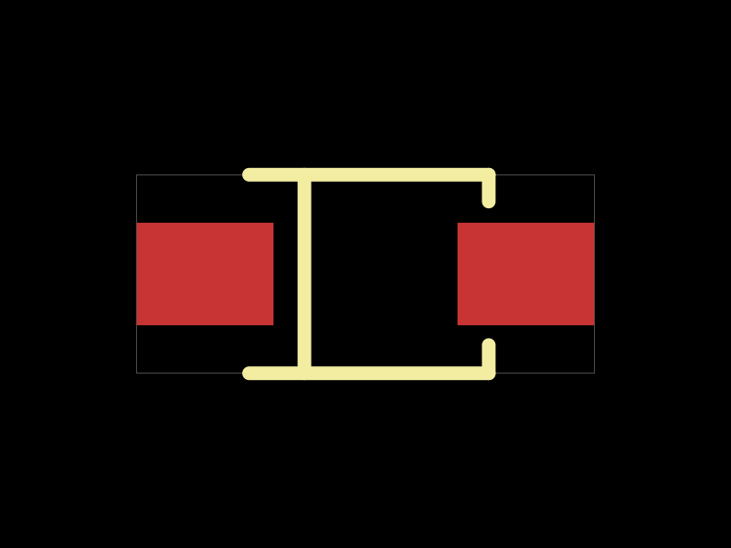
The ADS7841ESQDBQRQ1 is a 16-pin touchscreen controller IC with voltage, ground, communication, and mode control pins designed for interfacing with touch sensors.
# BOOSTXL-ADS7841-Q1 reconstruction

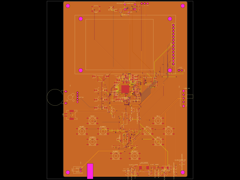
Native tscircuit reconstruction of TI's four-channel ADS7841-Q1 BoosterPack. The circuit and values follow TI user guide SNAU229 Figure 19 and its BOM. The design uses four meaningful schematic sheets because a literal one-sheet rendering was too dense to review safely.

## Current status

- Electrical source: matched to the TI BOM and schematic, including DNP options.
- Routing: 207 PCB traces, no jumpers, zero circuit-json DRC errors.
- Short check: `tsci check shorts --mode pcb --layer all` passes.
- Supply chain: JLCPCB/LCSC data is attached to every passive and imported production part. U1 REG71055DDCR (C2071120) and U2 TPS79901DRVR (C398922) are documented non-Q1 compatible substitutions for first-article use.
- Manufacturing release: approved for a **small first-article prototype order only**. See [docs/order-readiness.md](docs/order-readiness.md).

## Authoritative source

- Local: `reference/ti/BOOSTXL-ADS7841-Q1-user-guide-SNAU229.pdf`
- TI: <https://www.ti.com/lit/ug/snau229/snau229.pdf>
- BOM: Tables 1 and 2, pages 19–20.
- PCB reference: Figures 15–18, pages 20–23.
- Complete schematic: Figure 19, page 24.

## Verification

```sh
bun run typecheck
bun run build
bun run check:shorts
bun run check:release
```

The normal Gerber exporter currently rejects four-layer inner-layer output. `check:shorts` deliberately runs the CLI PCB checker separately on top and bottom at stable raster resolutions.

## Design rules

- Four copper layers
- 0.2 mm default signal trace width
- 0.3 mm minimum via hole
- 0.45 mm minimum via pad
- Bottom GND copper pour
- No explicit `<netlabel>` elements
- Native passives in `index.circuit.tsx`; imported JLC components only where a production part/footprint is required