ShiboSoftwareDev/usb-pd-quad-dc-motor-controller
USB‑C USB‑PD–powered ESP32‑C3 controller with protected data, 3.3‑V regulation, and dual DRV8847 H‑bridges driving four current-limited brushed DC motors with status indication and protection.
- Version
- 1.0.0
- License
- unset
- Stars
- 0
index.circuit.tsx
PCB
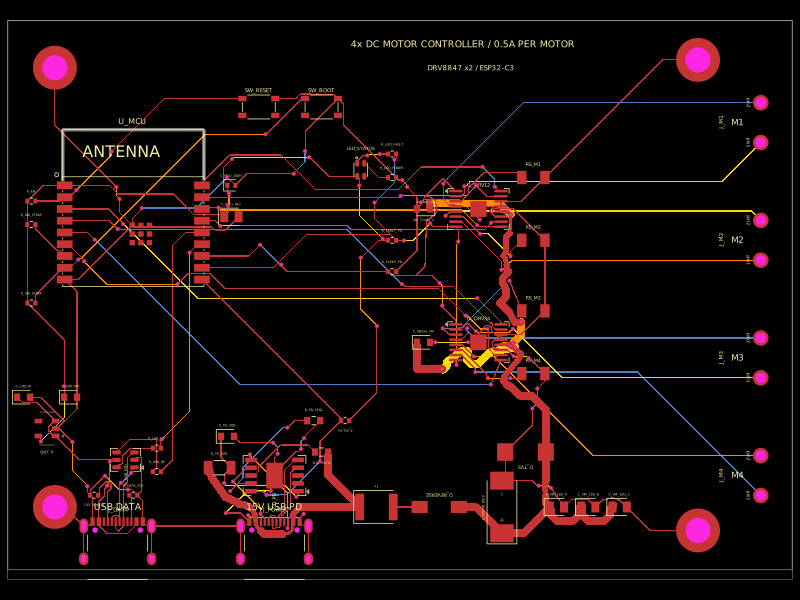
Schematic

import { AP2112K_3_3TRG1 } from "./imports/AP2112K_3_3TRG1"
import { CH224K } from "./imports/CH224K"
import { DRV8847PWPR } from "./imports/DRV8847PWPR"
import { ESP32_C3_WROOM_02_N4 } from "./imports/ESP32_C3_WROOM_02_N4"
import { HoLRT1206_1W_300mR_1_ } from "./imports/HoLRT1206_1W_300mR_1_"
import { LTST_C19HE1WT } from "./imports/LTST_C19HE1WT"
import { SKRPACE010 } from "./imports/SKRPACE010"
import { SMBJ16CAQ_13_F } from "./imports/SMBJ16CAQ_13_F"
import { SS54 } from "./imports/SS54"
import { TCJD107M025R0055E } from "./imports/TCJD107M025R0055E"
import { TYPE_C_16PIN_2MD_073_ } from "./imports/TYPE_C_16PIN_2MD_073_"
import { USBLC6_2SC6 } from "./imports/USBLC6_2SC6"
import { WJ500V_5_08_2P } from "./imports/WJ500V_5_08_2P"

const R = ({ jlcpcb, ...props }: any) => <resistor supplierPartNumbers={{ jlcpcb: [jlcpcb] }} {...props} />
const C = ({ jlcpcb, ...props }: any) => <capacitor supplierPartNumbers={{ jlcpcb: [jlcpcb] }} {...props} />

const MountingHole = ({ name, pcbX, pcbY }: any) => (
  <chip name={name} pcbX={pcbX} pcbY={pcbY} pinLabels={{ pin1: ["GND"] }} connections={{ pin1: "net.GND" }} footprint={<footprint><platedhole portHints={["pin1"]} shape="circle" holeDiameter="3.2mm" outerDiameter="5.6mm" /></footprint>} />
)

/** Four brushed-DC channels inspired by the Adafruit Motor Shield V2 architecture,
 * using two TI DRV8847 dual H-bridges and direct ESP32-C3 control. Each channel
 * is hardware-limited to about 0.5 A by a 0.30 ohm shunt (150 mV / 0.30 ohm).
 */
export default function UsbPdQuadDcMotorController() {
  return (
    <board width="100mm" height="70mm" layers={4} thickness="1.6mm" minViaHoleDiameter="0.3mm" minViaPadDiameter="0.55mm" autorouterVersion="beta_pipeline7" autorouterEffortLevel="2x">
      <net name="GND" />
      <net name="USB_5V" />
      <net name="V3V3" />
      <net name="USB_DM_CONN" />
      <net name="USB_DP_CONN" />
      <net name="USB_DM_ESD" />
      <net name="USB_DP_ESD" />
      <net name="PD_VBUS_RAW" />
      <net name="PD_DP" />
      <net name="PD_DM" />
      <net name="PD_VDD" />
      <net name="VMOTOR" />
      <net name="PD_POWER_GOOD" />
      <net name="DRIVERS_SLEEP" />
      <net name="DRIVERS_FAULT" />
      <net name="M1_IN1" />
      <net name="M1_IN2" />
      <net name="M2_IN1" />
      <net name="M2_IN2" />
      <net name="M3_IN1" />
      <net name="M3_IN2" />
      <net name="M4_IN1" />
      <net name="M4_IN2" />

      <TYPE_C_16PIN_2MD_073_ name="J_DATA" pcbX={-36} pcbY={-31} noConnect={["SBU1", "SBU2"]} connections={{ VBUS1: "net.USB_5V", VBUS2: "net.USB_5V", GND1: "net.GND", GND2: "net.GND", EH1: "net.GND", EH2: "net.GND", EH3: "net.GND", EH4: "net.GND", Dn1: "net.USB_DM_CONN", Dn2: "net.USB_DM_CONN", Dp1: "net.USB_DP_CONN", Dp2: "net.USB_DP_CONN" }} />
      <R name="R_DATA_CC1" resistance="5.1k" footprint="0402" jlcpcb="C25905" pcbX={-39} pcbY={-25.5} pcbRotation={180} connections={{ pin1: ".J_DATA > .CC1", pin2: "net.GND" }} />
      <R name="R_DATA_CC2" resistance="5.1k" footprint="0402" jlcpcb="C25905" pcbX={-34} pcbY={-25.5} connections={{ pin1: ".J_DATA > .CC2", pin2: "net.GND" }} />
      <USBLC6_2SC6 name="U_USB_ESD" pcbX={-35} pcbY={-21} pcbRotation={90} connections={{ pin1: "net.USB_DM_CONN", pin6: "net.USB_DM_ESD", pin3: "net.USB_DP_CONN", pin4: "net.USB_DP_ESD", VBUS: "net.USB_5V", GND: "net.GND" }} />
      <R name="R_USB_DM" resistance="22" footprint="0402" jlcpcb="C25092" pcbX={-31} pcbY={-19.5} connections={{ pin1: "net.USB_DM_ESD", pin2: ".U_MCU > .IO18" }} />
      <R name="R_USB_DP" resistance="22" footprint="0402" jlcpcb="C25092" pcbX={-31} pcbY={-22.5} connections={{ pin1: "net.USB_DP_ESD", pin2: ".U_MCU > .IO19" }} />

      <AP2112K_3_3TRG1 name="U_LDO" pcbX={-45} pcbY={-17} noConnect={["NC"]} connections={{ VIN: "net.USB_5V", EN: "net.USB_5V", VOUT: "net.V3V3", GND: "net.GND" }} />
      <C name="C_LDO_IN" capacitance="1uF" footprint="0603" jlcpcb="C15849" pcbX={-48} pcbY={-13} connections={{ pin1: "net.USB_5V", pin2: "net.GND" }} />
      <C name="C_LDO_OUT" capacitance="1uF" footprint="0603" jlcpcb="C15849" pcbX={-42} pcbY={-13} connections={{ pin1: "net.V3V3", pin2: "net.GND" }} />

      <ESP32_C3_WROOM_02_N4 name="U_MCU" pcbX={-34} pcbY={8} connections={{ "3V3": "net.V3V3", GND: "net.GND", EP: "net.GND", IO0: "net.M1_IN1", IO1: "net.M1_IN2", IO2: "net.M2_IN1", IO3: "net.M2_IN2", IO4: "net.M3_IN1", IO5: "net.M3_IN2", IO6: "net.M4_IN1", IO7: "net.M4_IN2", TXD: "net.DRIVERS_SLEEP", RXD: "net.DRIVERS_FAULT", IO10: "net.PD_POWER_GOOD" }} />
      <C name="C_MCU_100N" capacitance="100nF" footprint="0402" jlcpcb="C1525" pcbX={-21.5} pcbY={14} connections={{ pin1: "net.V3V3", pin2: "net.GND" }} />
      <C name="C_MCU_10U" capacitance="10uF" footprint="0805" jlcpcb="C15850" pcbX={-21.5} pcbY={10} connections={{ pin1: "net.V3V3", pin2: "net.GND" }} />
      <R name="R_EN" resistance="10k" footprint="0402" jlcpcb="C25744" pcbX={-47} pcbY={12} connections={{ pin1: "net.V3V3", pin2: ".U_MCU > .EN" }} />
      <SKRPACE010 name="SW_RESET" pcbX={-18} pcbY={24} noConnect={["pin3", "pin4"]} connections={{ pin1: ".U_MCU > .EN", pin2: "net.GND" }} />
      <R name="R_IO8_STRAP" resistance="10k" footprint="0402" jlcpcb="C25744" pcbX={-47} pcbY={9} connections={{ pin1: "net.V3V3", pin2: ".U_MCU > .IO8" }} />
      <R name="R_IO9_STRAP" resistance="10k" footprint="0402" jlcpcb="C25744" pcbX={-47} pcbY={-1} connections={{ pin1: "net.V3V3", pin2: ".U_MCU > .IO9" }} />
      <SKRPACE010 name="SW_BOOT" pcbX={-10} pcbY={24} noConnect={["pin3", "pin4"]} connections={{ pin1: ".U_MCU > .IO9", pin2: "net.GND" }} />

      <TYPE_C_16PIN_2MD_073_ name="J_POWER" pcbX={-16} pcbY={-31} noConnect={["SBU1", "SBU2"]} connections={{ VBUS1: "net.PD_VBUS_RAW", VBUS2: "net.PD_VBUS_RAW", GND1: "net.GND", GND2: "net.GND", EH1: "net.GND", EH2: "net.GND", EH3: "net.GND", EH4: "net.GND", Dn1: "net.PD_DM", Dn2: "net.PD_DM", Dp1: "net.PD_DP", Dp2: "net.PD_DP" }} />
      <CH224K name="U_PD" pcbX={-16} pcbY={-23} pcbRotation={90} noConnect={["CFG2", "CFG3"]} connections={{ DP: "net.PD_DP", DM: "net.PD_DM", CC1: ".J_POWER > .CC1", CC2: ".J_POWER > .CC2", VDD: "net.PD_VDD", GND: "net.GND", PG: "net.PD_POWER_GOOD" }} />
      <R name="R_PD_VDD" resistance="1k" footprint="1206" jlcpcb="C844867" manufacturerPartNumber="CRCW12061K00FKEAHP" pcbX={-23} pcbY={-22} connections={{ pin1: "net.PD_VBUS_RAW", pin2: "net.PD_VDD" }} />
      <C name="C_PD_VDD" capacitance="1uF" footprint="0603" jlcpcb="C15849" pcbX={-22} pcbY={-18} connections={{ pin1: "net.PD_VDD", pin2: "net.GND" }} />
      <R name="R_PD_VBUS" resistance="10k" footprint="0603" jlcpcb="C2906982" pcbX={-10} pcbY={-20} pcbRotation={180} connections={{ pin1: "net.PD_VBUS_RAW", pin2: ".U_PD > .VBUS" }} />
      <R name="R_PD_CFG1" resistance="56k" footprint="0603" jlcpcb="C23206" pcbX={-11} pcbY={-16} connections={{ pin1: ".U_PD > .CFG1", pin2: "net.GND" }} />
      <R name="R_PD_PG" resistance="10k" footprint="0402" jlcpcb="C25744" pcbX={-7} pcbY={-16} pcbRotation={180} connections={{ pin1: "net.V3V3", pin2: "net.PD_POWER_GOOD" }} />

      <fuse name="F1" currentRating="3A" voltageRating="30V" footprint="1812" supplierPartNumbers={{ jlcpcb: ["C48985875"] }} manufacturerPartNumber="1812L300/30GR" pcbX={-3} pcbY={-27} connections={{ pin1: "net.PD_VBUS_RAW" }} />
      <SS54 name="D_REVERSE" pcbX={5} pcbY={-27} pcbRotation={180} connections={{ anode: ".F1 > .pin2", cathode: "net.VMOTOR" }} />
      <TCJD107M025R0055E name="C_MOTOR_BULK" pcbX={13} pcbY={-27} pcbRotation={90} connections={{ pin1: "net.VMOTOR", pin2: "net.GND" }} />
      <C name="C_VM_10U_A" capacitance="10uF" footprint="0805" jlcpcb="C15850" pcbX={20} pcbY={-27} connections={{ pin1: "net.VMOTOR", pin2: "net.GND" }} />
      <C name="C_VM_10U_B" capacitance="10uF" footprint="0805" jlcpcb="C15850" pcbX={24} pcbY={-27} connections={{ pin1: "net.VMOTOR", pin2: "net.GND" }} />
      <C name="C_VM_10U_C" capacitance="10uF" footprint="0805" jlcpcb="C15850" pcbX={28} pcbY={-27} connections={{ pin1: "net.VMOTOR", pin2: "net.GND" }} />
      <SMBJ16CAQ_13_F name="D_TVS" pcbX={16} pcbY={-20} pcbRotation={180} connections={{ pin1: "net.VMOTOR", pin2: "net.GND" }} />

      <DRV8847PWPR name="U_DRV12" pcbX={10} pcbY={11} connections={{ nSLEEP: "net.DRIVERS_SLEEP", nFAULT: "net.DRIVERS_FAULT", IN1: "net.M1_IN1", IN2: "net.M1_IN2", IN3: "net.M2_IN1", IN4: "net.M2_IN2", OUT1: ".J_M1 > .pin1", OUT2: ".J_M1 > .pin2", OUT3: ".J_M2 > .pin1", OUT4: ".J_M2 > .pin2", ISEN12: ".RS_M1 > .pin1", ISEN34: ".RS_M2 > .pin1", TRQ: "net.GND", MODE: "net.GND", VM: "net.VMOTOR", GND: "net.GND", EP: "net.GND" }} />
      <C name="C_DRV12_VM" capacitance="100nF" footprint="0603" jlcpcb="C14663" pcbX={3} pcbY={11} pcbRotation={180} connections={{ pin1: "net.VMOTOR", pin2: "net.GND" }} />
      <HoLRT1206_1W_300mR_1_ name="RS_M1" pcbX={17} pcbY={15} connections={{ pin2: "net.GND" }} />
      <HoLRT1206_1W_300mR_1_ name="RS_M2" pcbX={17} pcbY={7} connections={{ pin2: "net.GND" }} />

      <DRV8847PWPR name="U_DRV34" pcbX={10} pcbY={-6} connections={{ nSLEEP: "net.DRIVERS_SLEEP", nFAULT: "net.DRIVERS_FAULT", IN1: "net.M3_IN1", IN2: "net.M3_IN2", IN3: "net.M4_IN1", IN4: "net.M4_IN2", OUT1: ".J_M3 > .pin1", OUT2: ".J_M3 > .pin2", OUT3: ".J_M4 > .pin1", OUT4: ".J_M4 > .pin2", ISEN12: ".RS_M3 > .pin1", ISEN34: ".RS_M4 > .pin1", TRQ: "net.GND", MODE: "net.GND", VM: "net.VMOTOR", GND: "net.GND", EP: "net.GND" }} />
      <C name="C_DRV34_VM" capacitance="100nF" footprint="0603" jlcpcb="C14663" pcbX={3} pcbY={-6} connections={{ pin1: "net.VMOTOR", pin2: "net.GND" }} />
      <HoLRT1206_1W_300mR_1_ name="RS_M3" pcbX={17} pcbY={-2} connections={{ pin2: "net.GND" }} />
      <HoLRT1206_1W_300mR_1_ name="RS_M4" pcbX={17} pcbY={-10} connections={{ pin2: "net.GND" }} />
      <R name="R_SLEEP_PD" resistance="100k" footprint="0402" jlcpcb="C25741" pcbX={-1} pcbY={3} connections={{ pin1: "net.DRIVERS_SLEEP", pin2: "net.GND" }} />
      <R name="R_FAULT_PU" resistance="10k" footprint="0402" jlcpcb="C25744" pcbX={-1} pcbY={7} connections={{ pin1: "net.V3V3", pin2: "net.DRIVERS_FAULT" }} />

      <WJ500V_5_08_2P name="J_M1" pcbX={46} pcbY={22} pcbRotation={90} />
      <WJ500V_5_08_2P name="J_M2" pcbX={46} pcbY={7} pcbRotation={90} />
      <WJ500V_5_08_2P name="J_M3" pcbX={46} pcbY={-8} pcbRotation={90} />
      <WJ500V_5_08_2P name="J_M4" pcbX={46} pcbY={-23} pcbRotation={90} />

      <LTST_C19HE1WT name="LED_STATUS" pcbX={-5} pcbY={16} noConnect={["B_NEG"]} connections={{ _POS: "net.V3V3" }} />
      <R name="R_LED_FAULT" resistance="1k" footprint="0402" jlcpcb="C11702" pcbX={-1} pcbY={18} connections={{ pin1: ".LED_STATUS > .R_NEG", pin2: "net.DRIVERS_FAULT" }} />
      <R name="R_LED_POWER" resistance="1k" footprint="0402" jlcpcb="C11702" pcbX={-1} pcbY={15} connections={{ pin1: ".LED_STATUS > .G_NEG", pin2: "net.GND" }} />

      <trace name="PD_INPUT_HEAVY" from=".J_POWER > .VBUS1" to=".F1 > .pin1" thickness="1mm" />
      <trace name="FUSE_TO_DIODE_HEAVY" from=".F1 > .pin2" to=".D_REVERSE > .anode" thickness="1mm" />
      <trace name="VMOTOR_HEAVY" from=".D_REVERSE > .cathode" to="net.VMOTOR" thickness="1mm" />
      <trace name="M1_OUT_A" from=".U_DRV12 > .OUT1" to=".J_M1 > .pin1" thickness="0.8mm" />
      <trace name="M1_OUT_B" from=".U_DRV12 > .OUT2" to=".J_M1 > .pin2" thickness="0.8mm" />
      <trace name="M2_OUT_A" from=".U_DRV12 > .OUT3" to=".J_M2 > .pin1" thickness="0.8mm" />
      <trace name="M2_OUT_B" from=".U_DRV12 > .OUT4" to=".J_M2 > .pin2" thickness="0.8mm" />
      <trace name="M3_OUT_A" from=".U_DRV34 > .OUT1" to=".J_M3 > .pin1" thickness="0.8mm" />
      <trace name="M3_OUT_B" from=".U_DRV34 > .OUT2" to=".J_M3 > .pin2" thickness="0.8mm" />
      <trace name="M4_OUT_A" from=".U_DRV34 > .OUT3" to=".J_M4 > .pin1" thickness="0.8mm" />
      <trace name="M4_OUT_B" from=".U_DRV34 > .OUT4" to=".J_M4 > .pin2" thickness="0.8mm" />

      <MountingHole name="MH1" pcbX={-44} pcbY={29} />
      <MountingHole name="MH2" pcbX={38} pcbY={30} />
      <MountingHole name="MH3" pcbX={-44} pcbY={-27} />
      <MountingHole name="MH4" pcbX={38} pcbY={-30} />
      <silkscreentext text="USB DATA" pcbX={-36} pcbY={-27} fontSize="1.2mm" />
      <silkscreentext text="15V USB-PD" pcbX={-16} pcbY={-27} fontSize="1.2mm" />
      <silkscreentext text="4x DC MOTOR CONTROLLER / 0.5A PER MOTOR" pcbX={8} pcbY={32} fontSize="1.2mm" />
      <silkscreentext text="M1" pcbX={43} pcbY={22} fontSize="1.1mm" />
      <silkscreentext text="M2" pcbX={43} pcbY={7} fontSize="1.1mm" />
      <silkscreentext text="M3" pcbX={43} pcbY={-8} fontSize="1.1mm" />
      <silkscreentext text="M4" pcbX={43} pcbY={-23} fontSize="1.1mm" />
      <silkscreentext text="DRV8847 x2 / ESP32-C3" pcbX={9} pcbY={29} fontSize="0.9mm" />
    </board>
  )
}
Related Packages
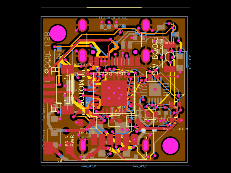 More from this authorShiboSoftwareDev/nema8-20mm-usbc-pd-controllerA 20×20 mm four-layer USB‑C PD stepper motor controller PCB using a CH32X035 MCU, TMC2209 driver, protected power inputs, USB data/boot interface, 3.3 V regulation, ESD/TVS protection, current-sense circuitry, and NEMA‑8 motor outputs.
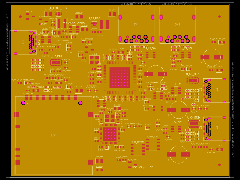 Similar packagegokul/usb3-sd-hubEngineering draft: four-layer, computer-powered USB 3 hub with one USB-C host socket, two USB-C and two USB-A accessory sockets, and a full-size SD slot. Board and three schematic previews are available. Routing and production checks are incomplete; not fabrication ready.
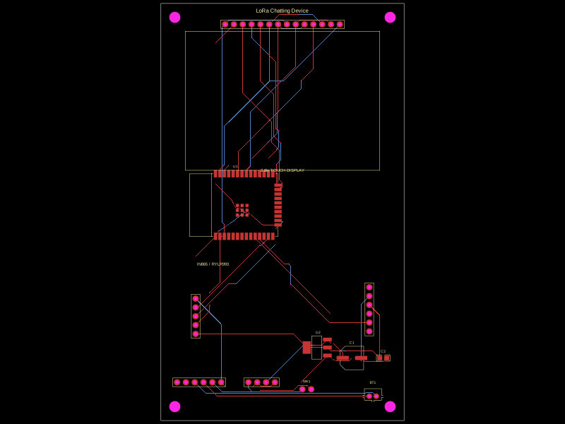 Discover something newhrithik18k/Chatting-DeviceThis code defines React components representing surface-mount voltage regulator and resistor chips with specified pin layouts, footprints, and 3D CAD models for electronic hardware design.