ShiboSoftwareDev/solar-battery-charger
This code defines various surface-mount and through-hole electronic components (like diodes, voltage regulators, and ICs) with detailed footprints, 3D models, and pin configurations for PCB design.
- Version
- 1.0.2
- License
- unset
- Stars
- 0
imports/MCP73113T_06SI_MF.tsx
import type { ChipProps } from "@tscircuit/props"

const pinLabels = {
  pin1: ["VDD1"],
  pin2: ["VDD2"],
  pin3: ["VBAT1"],
  pin4: ["VBAT2"],
  pin5: ["NC1"],
  pin6: ["NC2"],
  pin7: ["STAT"],
  pin8: ["VSS1"],
  pin9: ["VSS2"],
  pin10: ["PROG"],
  pin11: ["EP"]
} as const

export const MCP73113T_06SI_MF = (props: ChipProps<typeof pinLabels>) => {
  return (
    <chip
      pinLabels={pinLabels}
      supplierPartNumbers={{
  "jlcpcb": [
    "C623827"
  ]
}}
      manufacturerPartNumber="MCP73113T_06SI_MF"
      footprint={<footprint>
        <smtpad portHints={["pin1"]} pcbX="-1.407414mm" pcbY="0.999998mm" width="0.6649974mm" height="0.2800096mm" shape="rect" />
<smtpad portHints={["pin2"]} pcbX="-1.407414mm" pcbY="0.499872mm" width="0.6649974mm" height="0.2800096mm" shape="rect" />
<smtpad portHints={["pin3"]} pcbX="-1.407414mm" pcbY="0mm" width="0.6649974mm" height="0.2800096mm" shape="rect" />
<smtpad portHints={["pin4"]} pcbX="-1.407414mm" pcbY="-0.500126mm" width="0.6649974mm" height="0.2800096mm" shape="rect" />
<smtpad portHints={["pin5"]} pcbX="-1.407414mm" pcbY="-0.999998mm" width="0.6649974mm" height="0.2800096mm" shape="rect" />
<smtpad portHints={["pin6"]} pcbX="1.407414mm" pcbY="-0.999998mm" width="0.6649974mm" height="0.2800096mm" shape="rect" />
<smtpad portHints={["pin7"]} pcbX="1.407414mm" pcbY="-0.500126mm" width="0.6649974mm" height="0.2800096mm" shape="rect" />
<smtpad portHints={["pin8"]} pcbX="1.407414mm" pcbY="0mm" width="0.6649974mm" height="0.2800096mm" shape="rect" />
<smtpad portHints={["pin9"]} pcbX="1.407414mm" pcbY="0.499872mm" width="0.6649974mm" height="0.2800096mm" shape="rect" />
<smtpad portHints={["pin10"]} pcbX="1.407414mm" pcbY="0.999998mm" width="0.6649974mm" height="0.2800096mm" shape="rect" />
<smtpad portHints={["pin11"]} pcbX="0mm" pcbY="0mm" width="1.6400018mm" height="2.3800054mm" shape="rect" />
<silkscreenpath route={[{"x":-1.5761969999999934,"y":1.5761969999999934},{"x":1.5761969999999792,"y":1.5761969999999934}]} />
<silkscreenpath route={[{"x":-1.5761969999999934,"y":-1.5761969999999934},{"x":1.5761969999999792,"y":-1.5761969999999934}]} />
<silkscreentext text="{NAME}" pcbX="-0.1397mm" pcbY="2.6256mm" anchorAlignment="center" fontSize="1mm" />
<courtyardoutline outline={[{"x":-2.2565999999999917,"y":1.8756000000000057},{"x":1.9772000000000105,"y":1.8756000000000057},{"x":1.9772000000000105,"y":-1.8247999999999962},{"x":-2.2565999999999917,"y":-1.8247999999999962},{"x":-2.2565999999999917,"y":1.8756000000000057}]} />
      </footprint>}
      cadModel={{
        objUrl: "https://modelcdn.tscircuit.com/easyeda_models/assets/C623827.obj?uuid=c995bf3d85654ebb8e160662de6e24f5",
        stepUrl: "https://modelcdn.tscircuit.com/easyeda_models/assets/C623827.step?uuid=c995bf3d85654ebb8e160662de6e24f5",
        pcbRotationOffset: 0,
        modelOriginPosition: { x: 0, y: 0, z: -0.05 },
      }}
      {...props}
    />
  )
}
Related Packages
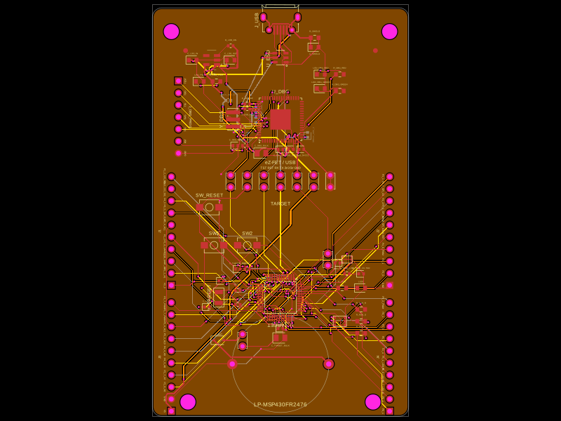 More from this authorShiboSoftwareDev/lp-msp430fr2476This design implements a microcontroller-based development board featuring an MSP430FR2476 target MCU with associated power regulation, USB host interface with ESD protection, multiple headers for peripherals and BoosterPacks, and integrated status LEDs and sensors.
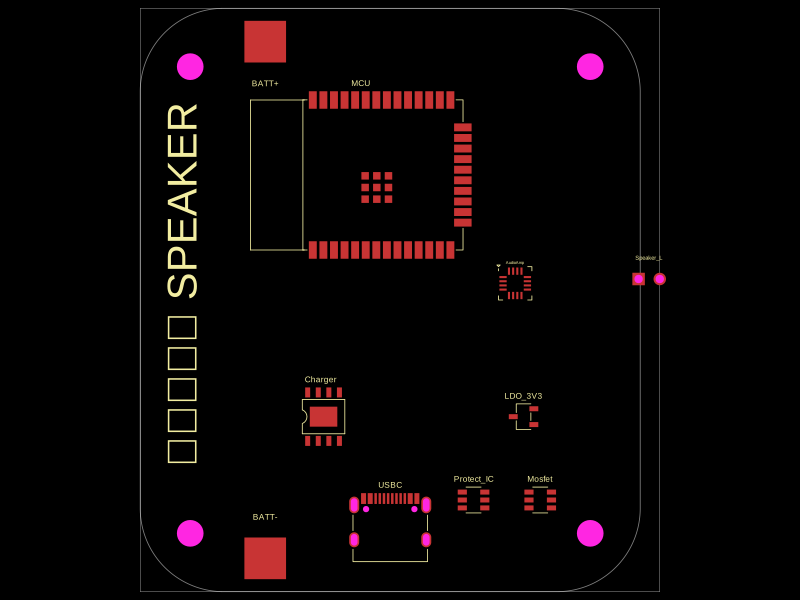 Similar packagemohan-bee/speakerThis code defines configurable 3D models and PCB footprints for various electronic components, including a battery charger IC, a dual Hall sensor, a dual power switch, and a voltage regulator, with detailed pinouts, footprints, and CAD models for schematic and physical design.