ShiboSoftwareDev/solar-battery-charger
This code defines various surface-mount and through-hole electronic components (like diodes, voltage regulators, and ICs) with detailed footprints, 3D models, and pin configurations for PCB design.
- Version
- 1.0.2
- License
- unset
- Stars
- 0
REPROS.md
# Repros for IC1 Routing Issues

These are intended as small starting points for `@tscircuit/core` regression tests.
They avoid explicit `pcbPath` coordinates and focus on routing input/output behavior.

## 1. Explicit trace thickness is clamped by board min trace width

### Problem

Two explicit traces connect pads to the same net and both request `0.06mm`.
The generated source traces preserve `min_trace_thickness: 0.06`, but the emitted
PCB route is widened to the board/router minimum, e.g. `0.15mm`.

On the solar charger board this is the `IC1.B2 -> net.SCL` and
`J4.SCL -> net.SCL` connection. The center pad trace is visually thick even
though both source traces specify `thickness="0.06mm"`.

### Reduced JSX

```tsx
import React from "react"

const OnePad = ({ name, pcbX, pcbY }: { name: string; pcbX: number; pcbY: number }) => (
  <chip
    name={name}
    pcbX={pcbX}
    pcbY={pcbY}
    pinLabels={{ pin1: ["P"] }}
    footprint={
      <footprint>
        <smtpad
          portHints={["pin1", "P"]}
          pcbX="0mm"
          pcbY="0mm"
          width="0.25mm"
          height="0.25mm"
          shape="rect"
        />
      </footprint>
    }
  />
)

export default () => (
  <board width="20mm" height="10mm" minTraceWidth="0.15mm">
    <OnePad name="U1" pcbX={-4} pcbY={0} />
    <OnePad name="J1" pcbX={4} pcbY={0} />

    <trace from="U1.P" to="net.SCL" thickness="0.06mm" />
    <trace from="J1.P" to="net.SCL" thickness="0.06mm" />
  </board>
)
```

### Expected

The single routed `net.SCL` PCB trace should use the explicit net trace width:

```ts
expect(uniqueWireWidthsForNet("SCL")).toEqual([0.06])
```

### Actual symptom

The route is emitted at the board/router minimum:

```ts
expect(uniqueWireWidthsForNet("SCL")).toEqual([0.15])
```

### Why this looks like core

`source_trace.min_trace_thickness` is correctly present. The issue appears when
core creates/applies routing connections: the net route width gets clamped by
the board minimum instead of preserving the explicit trace thickness.

Relevant behavior observed in local `@tscircuit/core`:

- source traces carry `min_trace_thickness: 0.06`
- net routing connection initially sees `width: 0.06`
- DRC/min-width application raises it to the board/router minimum

The desired behavior is probably: explicit `trace.thickness` should be a route
width request for that connection, while board `minTraceWidth` should be a DRC
constraint or fallback, not an override for explicit narrow traces.

## 2. Multi-port net emits an orphan/cut trace segment

### Problem

A multi-port net can emit an extra PCB trace fragment with no real source trace
and no port-connected endpoints. On the solar charger board this appears as a
short cut segment at the bottom right:

```txt
Trace [trace[source_net_29_mst1_0]] has disconnected endpoint at (-5.70, -12.55)
Trace [trace[source_net_29_mst1_0]] has disconnected endpoint at (-5.28, -12.55)
```

In the generated circuit JSON, the bad fragment looked like:

```json
{
  "type": "pcb_trace",
  "pcb_trace_id": "source_net_29_mst1_0",
  "connection_name": "source_net_29",
  "source_trace_id": undefined,
  "route": [
    { "route_type": "wire", "x": -5.7, "y": -12.55002, "width": 0.1, "layer": "top" },
    { "route_type": "wire", "x": -5.281, "y": -12.55002, "width": 0.1, "layer": "top" }
  ]
}
```

### Reduced JSX

This reproduces the same shape of input: four independent stubs into one net,
with three local output-stage pads and one far connector pad.

```tsx
import React from "react"

const OnePad = ({ name, pcbX, pcbY }: { name: string; pcbX: number; pcbY: number }) => (
  <chip
    name={name}
    pcbX={pcbX}
    pcbY={pcbY}
    pinLabels={{ pin1: ["P"] }}
    footprint={
      <footprint>
        <smtpad
          portHints={["pin1", "P"]}
          pcbX="0mm"
          pcbY="0mm"
          width="1mm"
          height="1mm"
          shape="rect"
        />
      </footprint>
    }
  />
)

export default () => (
  <board width="34.8mm" height="30mm" autorouterVersion="v4">
    <OnePad name="U1_OUTPUT" pcbX={0.495} pcbY={-13.25} />
    <OnePad name="L2_OUT" pcbX={-8.4} pcbY={-12.205} />
    <OnePad name="C_VOLT2_POS" pcbX={-5.5} pcbY={-10.857} />
    <OnePad name="J2_VOUT" pcbX={16} pcbY={11.3} />

    <trace from="U1_OUTPUT.P" to="net.VOUT" />
    <trace from="L2_OUT.P" to="net.VOUT" />
    <trace from="C_VOLT2_POS.P" to="net.VOUT" />
    <trace from="J2_VOUT.P" to="net.VOUT" />
  </board>
)
```

### Expected

All emitted PCB traces for `net.VOUT` should have at least one source trace or
valid port endpoint ownership, and there should be no disconnected-endpoint
errors:

```ts
const voutTraces = getPcbTracesForNet("VOUT")

expect(voutTraces.every((trace) => trace.source_trace_id)).toBe(true)
expect(errors.map((e) => e.message)).not.toContain("disconnected endpoint")
```

More directly, no emitted route should be just an unanchored two-point wire:

```ts
expect(
  voutTraces.some(
    (trace) =>
      !trace.source_trace_id &&
      trace.route.length === 2 &&
      !trace.route.some((p) => p.start_pcb_port_id || p.end_pcb_port_id),
  ),
).toBe(false)
```

### Actual symptom

On the solar charger board, the router/core output includes an orphan route
similar to:

```ts
{
  pcb_trace_id: "source_net_29_mst1_0",
  source_trace_id: undefined,
  route: [
    { x: -5.70, y: -12.55, width: 0.1, layer: "top" },
    { x: -5.28, y: -12.55, width: 0.1, layer: "top" },
  ],
}
```

### Where to look

This may be autorouter output or core route-output conversion:

- If the autorouter output already contains the orphan two-point segment, fix
  the autorouter.
- If autorouter output is clean and core creates `source_net_29_mst1_0` while
  converting to `pcb_trace`, fix core.

The core-side regression test should capture the simple-route-json sent to the
autorouter and the route result before conversion, then assert where the orphan
first appears.
Related Packages
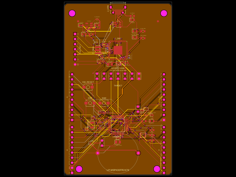 More from this authorShiboSoftwareDev/lp-msp430fr2476This design implements a microcontroller-based development board featuring an MSP430FR2476 target MCU with associated power regulation, USB host interface with ESD protection, multiple headers for peripherals and BoosterPacks, and integrated status LEDs and sensors.
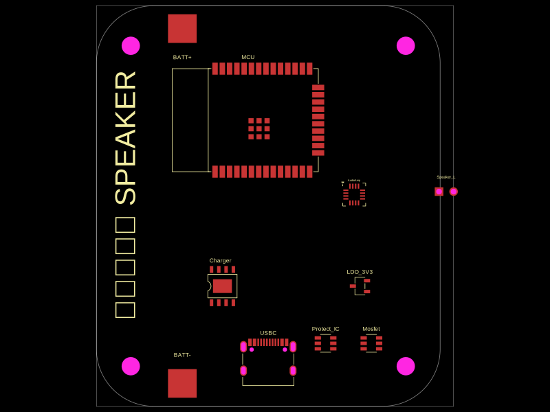 Similar packagemohan-bee/speakerThis code defines configurable 3D models and PCB footprints for various electronic components, including a battery charger IC, a dual Hall sensor, a dual power switch, and a voltage regulator, with detailed pinouts, footprints, and CAD models for schematic and physical design.