ShiboSoftwareDev/solar-battery-charger
This code defines various surface-mount and through-hole electronic components (like diodes, voltage regulators, and ICs) with detailed footprints, 3D models, and pin configurations for PCB design.
- Version
- 1.0.2
- License
- unset
- Stars
- 0
AUTOROUTING_PHASE_WIDTH_REPRO.md
# Autorouting phase + per-trace width repro

## Goal

Route the `IC1.B2 -> net.SCL` connection in its own autorouting phase with a narrow trace width, so the center pad on `IC1` has more clearance from nearby pads/traces.

The current circuit source can express the requested width, but the emitted PCB route still uses the default `0.15mm` wire width.

## Circuit change to reproduce

In `index.circuit.tsx`, add a targeted autorouting phase:

```tsx
<autoroutingphase phaseIndex={1} connections={["IC1.B2"]} />
```

Then change the center-pad trace from:

```tsx
<trace from="IC1.B2" to="net.SCL" />
```

to:

```tsx
<trace
  name="IC1_B2_SCL_CENTER_PAD"
  from="IC1.B2"
  to="net.SCL"
  routingPhaseIndex={1}
  width="0.06mm"
/>
```

Do not edit `standalone.circuit.tsx`.

## Repro steps

```bash
bun run typecheck
bun run build
```

Then inspect the generated circuit JSON:

```bash
node -e 'const fs=require("fs"); const j=JSON.parse(fs.readFileSync("dist/index/circuit.json","utf8")); const st=j.find(e=>e.type==="source_trace" && e.name==="IC1_B2_SCL_CENTER_PAD"); const pt=st && j.find(e=>e.type==="pcb_trace" && e.source_trace_id===st.source_trace_id); console.log(JSON.stringify({source_trace:st, pcb_widths:[...new Set((pt?.route||[]).filter(p=>p.route_type==="wire").map(p=>p.width))], pcb_trace_id:pt?.pcb_trace_id}, null, 2));'
```

## Current result

The source trace records the requested width:

```json
{
  "name": "IC1_B2_SCL_CENTER_PAD",
  "min_trace_thickness": 0.06
}
```

But the emitted PCB trace still uses:

```json
{
  "pcb_widths": [0.15]
}
```

The build also still reports IC1 center-pad clearance/overlap warnings such as:

```txt
PCB trace trace[.IC1 > port.pin5, .J4 > port.pin1] overlaps with pcb_smtpad "pcb_port[.IC1 > .A2]" (accidental contact)
```

## Expected result

The emitted `pcb_trace.route[]` wire points for the `IC1_B2_SCL_CENTER_PAD` route should use the requested width:

```json
{
  "pcb_widths": [0.06]
}
```

## Core behavior to check

Autorouting phase order is numeric ascending, with unphased routes last:

```txt
phaseIndex 0
phaseIndex 1
phaseIndex 10
unphased/null
```

So `phaseIndex={1}` only means this trace has its own phase. It does not mean it routes after unphased traces.

The width issue is separate: the requested per-trace width reaches `source_trace.min_trace_thickness`, but does not reach the final emitted `pcb_trace.route[].width`.

## Suggested core fix direction

When converting autorouter output traces back into circuit JSON PCB traces:

1. Match each routed trace back to its input `SimpleRouteConnection` by `connection_name`, `source_trace_id`, or `pcb_trace_id`.
2. Read `connection.nominalTraceWidth ?? connection.width`.
3. Apply that requested width to emitted `wire` route points.
4. Preserve that width for converted `through_obstacle -> through_pad` route points.

Also avoid clamping phase-specific connection width upward with `Math.max(...)` when the user explicitly requested a narrower connection width.
Related Packages
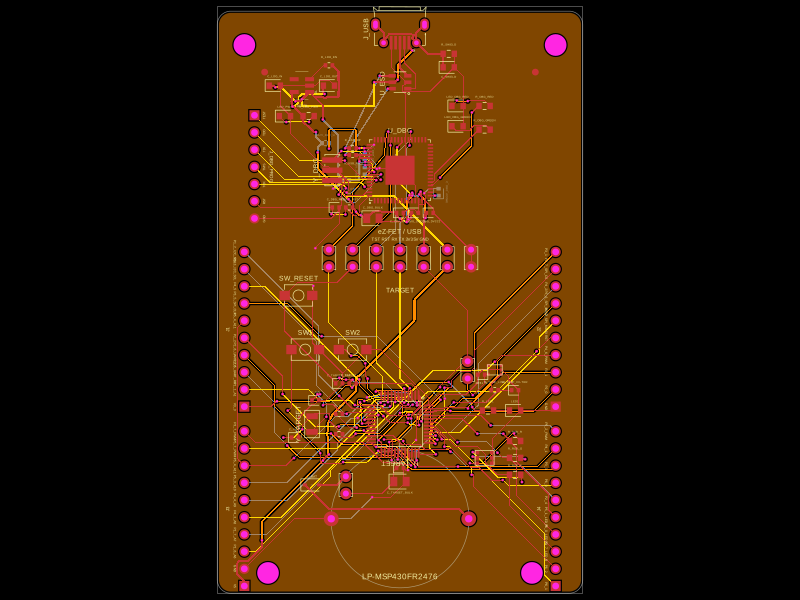 More from this authorShiboSoftwareDev/lp-msp430fr2476This design implements a microcontroller-based development board featuring an MSP430FR2476 target MCU with associated power regulation, USB host interface with ESD protection, multiple headers for peripherals and BoosterPacks, and integrated status LEDs and sensors.
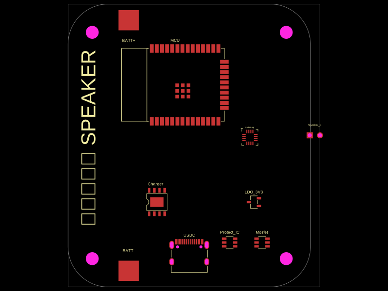 Similar packagemohan-bee/speakerThis code defines configurable 3D models and PCB footprints for various electronic components, including a battery charger IC, a dual Hall sensor, a dual power switch, and a voltage regulator, with detailed pinouts, footprints, and CAD models for schematic and physical design.