ShiboSoftwareDev/mspm0g3507-usb-c-dev-board
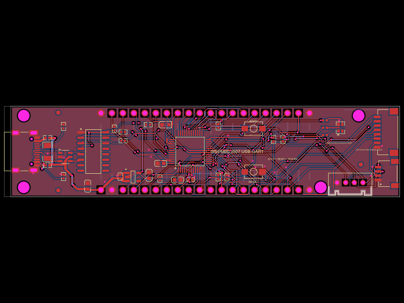
This circuit features a USB Type-C connector with integrated resistors and passives, a USB ESD protection device, a CH340 USB-to-serial interface chip, a 3.3V regulator (AP2112K), multiple decoupling and bulk capacitors, and a Microcontroller (MSPM0G3507) with associated I2C and SPI connections, providing USB communication, power regulation, and RGB LED control.
- Version
- 1.4.1
- License
- unset
- Stars
- 0
index.circuit.tsx
PCB
Schematic

import { AP2112K_3_3TRG1 } from "./imports/AP2112K_3_3TRG1"
import { A_0402WGF0000TCE } from "./imports/A_0402WGF0000TCE"
import { A_0402WGF1001TCE } from "./imports/A_0402WGF1001TCE"
import { A_0402WGF1002TCE } from "./imports/A_0402WGF1002TCE"
import { A_0402WGF3300TCE } from "./imports/A_0402WGF3300TCE"
import { A_0402WGF4701TCE } from "./imports/A_0402WGF4701TCE"
import { A_0402WGF4702TCE } from "./imports/A_0402WGF4702TCE"
import { A_0402WGF5101TCE } from "./imports/A_0402WGF5101TCE"
import { A_1206W4F0000T5E } from "./imports/A_1206W4F0000T5E"
import { CH340C } from "./imports/CH340C"
import { CL05B103KB5NNNC } from "./imports/CL05B103KB5NNNC"
import { CL05B104KO5NNNC } from "./imports/CL05B104KO5NNNC"
import { CL10A106KP8NNNC } from "./imports/CL10A106KP8NNNC"
import { CL10A475KO8NNNC } from "./imports/CL10A475KO8NNNC"
import { CL10B474KA8NNNC } from "./imports/CL10B474KA8NNNC"
import { MSPM0G3507SPTR } from "./imports/MSPM0G3507SPTR"
import { SM04B_SRSS_TB_LF__SN_ } from "./imports/SM04B_SRSS_TB_LF__SN_"
import { SM08B_SRSS_TB_LF__SN_ } from "./imports/SM08B_SRSS_TB_LF__SN_"
import { SZYY1615RGB_A_4pin } from "./imports/SZYY1615RGB_A_4pin"
import { TS342A2P_WZ } from "./imports/TS342A2P_WZ"
import { TYPE_C_31_M_12 } from "./imports/TYPE_C_31_M_12"
import { USBLC6_2SC6 } from "./imports/USBLC6_2SC6"
import { XL_1608SYGC_06 } from "./imports/XL_1608SYGC_06"
import { ZX_HY2_0_4PZZ } from "./imports/ZX_HY2_0_4PZZ"

const jlc = (partNumber: string) => ({ jlcpcb: [partNumber] })
const cleanComponentSilk = {
  pcbSx: { "& silkscreentext": { visibility: "hidden" as const } },
}

const MAIN_SCHEMATIC_SHEET = "MAIN"
const schematicSections = {
  usbConnector: "USB_CONNECTOR",
  usbUart: "USB_UART",
  power: "POWER",
  mcu: "MCU_CONTROL",
  rgb: "RGB_DEBUG",
  i2c: "I2C",
  spi: "SPI",
  headers: "HEADERS",
} as const

const schematicSectionStyle = (schSectionName: string) => ({
  ...cleanComponentSilk,
  schSectionName,
})

const HeaderPad = ({ index }: { index: number }) => (
  <platedhole
    name={`HEADER_PAD_${index + 1}`}
    portHints={[`pin${index + 1}`]}
    pcbX={`${(index - 9.5) * 2.54}mm`}
    pcbY="0mm"
    shape="circular_hole_with_rect_pad"
    holeDiameter="1.05mm"
    rectPadWidth="1.6mm"
    rectPadHeight="1.6mm"
    rectBorderRadius="0.8mm"
  />
)

const headerFootprint = (
  <footprint>
    {Array.from({ length: 20 }, (_, index) => (
      <HeaderPad key={`header-pad-${index + 1}`} index={index} />
    ))}
    <courtyardrect width="50.56mm" height="2.3mm" />
  </footprint>
)

const topHeaderPins = [
  "GND", "PA27", "PA26", "PA25", "PA24", "PA23", "PA22", "PA21",
  "PA20_SWCLK", "PA19_SWDIO", "PA18_BSL_INVOKE", "PA17", "PA16",
  "PA15", "PA14", "PA13", "PA12", "MCU_RESET_N", "VDD_3V3", "GND",
] as const

const bottomHeaderPins = [
  "VBUS_5V", "GND", "VDD_3V3", "PA0_I2C_SDA", "PA1_I2C_SCL",
  "PA2", "PA3", "PA4", "PA5", "PA6", "PA7", "PA8_SPI_DC",
  "PA9_SPI_RST", "PA10_UART_TX", "PA11_UART_RX", "PB6_SPI_CS",
  "PB7_SPI_MISO", "PB8_SPI_MOSI", "PB9_SPI_SCK", "GND",
] as const

const topSilkLabels = [
  "1 GND", "2 PA27", "3 PA26", "4 PA25", "5 PA24", "6 PA23",
  "7 PA22", "8 PA21", "9 SWCLK", "10 SWDIO", "11 BOOT/PA18",
  "12 PA17", "13 PA16", "14 PA15", "15 PA14", "16 PA13", "17 PA12",
  "18 RESET", "19 3V3", "20 GND",
] as const

const bottomSilkLabels = [
  "1 VBUS", "2 GND", "3 3V3", "4 SDA/PA0", "5 SCL/PA1", "6 PA2",
  "7 PA3", "8 PA4", "9 PA5", "10 PA6", "11 PA7", "12 DC/PA8",
  "13 RST/PA9", "14 TX/PA10", "15 RX/PA11", "16 CS/PB6",
  "17 MISO/PB7", "18 MOSI/PB8", "19 SCK/PB9", "20 GND",
] as const

const mcuBreakoutNets = [
  ["PA0", "PA0_I2C_SDA"], ["PA1", "PA1_I2C_SCL"], ["PA2", "PA2"],
  ["PA3", "PA3"], ["PA4", "PA4"], ["PA5", "PA5"], ["PA6", "PA6"],
  ["PA7", "PA7"], ["PA8", "PA8_SPI_DC"], ["PA9", "PA9_SPI_RST"],
  ["PA10", "PA10_UART_TX"], ["PA11", "PA11_UART_RX"],
  ["PB2", "PB2_RGB_RED"], ["PB3", "PB3_RGB_GREEN"],
  ["PB6", "PB6_SPI_CS"], ["PB7", "PB7_SPI_MISO"],
  ["PB8", "PB8_SPI_MOSI"], ["PB9", "PB9_SPI_SCK"],
  ["PB14", "PB14_RGB_BLUE"],
  ["PA12", "PA12"], ["PA13", "PA13"], ["PA14", "PA14"],
  ["PA15", "PA15"], ["PA16", "PA16"], ["PA17", "PA17"],
  ["PA18", "PA18_BSL_INVOKE"], ["PA19", "PA19_SWDIO"],
  ["PA20", "PA20_SWCLK"], ["PA21", "PA21"], ["PA22", "PA22"],
  ["PA23", "PA23"], ["PA24", "PA24"], ["PA25", "PA25"],
  ["PA26", "PA26"], ["PA27", "PA27"],
] as const

const headerNet = (label: string) => label === "GND" ? "net.GND" : `net.${label}`

const HeaderSilkLabel = ({ text, x, y }: { text: string, x: number, y: number }) => (
  <silkscreentext text={text} pcbX={x} pcbY={y} pcbRotation={90} fontSize="0.48mm" anchorAlignment="center" layer="bottom" />
)

const NamedTrace = ({ name, from, to }: { name: string, from: string, to: string }) => (
  <trace name={name} from={from} to={to} />
)

export default function MSPM0G3507UsbCDevBoard() {
  return (
    <board
      title="MSPM0G3507 USB-C Dev Board"
      outline={[
        { x: -45, y: 10.5 },
        { x: 45, y: 10.5 },
        { x: 45, y: -10.5 },
        { x: -45, y: -10.5 },
      ]}
      layers={2}
      schSheetName={MAIN_SCHEMATIC_SHEET}
      schY={10}
      schAutoLayoutEnabled
      minViaHoleDiameter="0.3mm"
      minViaPadDiameter="0.45mm"
      minViaEdgeToPadEdgeClearance="0.2mm"
    >
      <schematicsheet
        name={MAIN_SCHEMATIC_SHEET}
        displayName="MSPM0G3507 USB-C Development Board"
        sheetSize="ANSI_B"
        sheetWidth="431.8mm"
        sheetHeight="279.4mm"
      >
        <schematicsection name={schematicSections.usbConnector} displayName="USB-C receptacle & CC" sectionTitleFontSize="0.35mm" />
        <schematicsection name={schematicSections.usbUart} displayName="USB protection & UART bridge" sectionTitleFontSize="0.35mm" />
        <schematicsection name={schematicSections.power} displayName="5 V to 3.3 V power" sectionTitleFontSize="0.35mm" />
        <schematicsection name={schematicSections.mcu} displayName="MCU, reset & boot" sectionTitleFontSize="0.35mm" />
        <schematicsection name={schematicSections.rgb} displayName="RGB debug LED" sectionTitleFontSize="0.35mm" />
        <schematicsection name={schematicSections.i2c} displayName="I2C connectors" sectionTitleFontSize="0.35mm" />
        <schematicsection name={schematicSections.spi} displayName="SPI display connector" sectionTitleFontSize="0.35mm" />
        <schematicsection name={schematicSections.headers} displayName="GPIO & debug headers" sectionTitleFontSize="0.35mm" />
      </schematicsheet>

      <TYPE_C_31_M_12
        {...schematicSectionStyle(schematicSections.usbConnector)}
        name="J_USB_C"
        noConnect={["A8", "B8"]}
        obstructsWithinBounds={false}
        pcbX={-41.1}
        pcbY={0}
        pcbRotation={-90}
        schX={-12.78}
        schY={-4.45}
      />
      <A_1206W4F0000T5E {...schematicSectionStyle(schematicSections.usbConnector)} name="R_USB_DM_JOIN" pcbX={-36.5} pcbY={-0.1} pcbRotation={90} obstructsWithinBounds={false} schX={-14.65} schY={-6.69} />
      <A_0402WGF0000TCE {...schematicSectionStyle(schematicSections.usbConnector)} name="R_VBUS_A_LINK" pcbX={-36.5} pcbY={3.2} obstructsWithinBounds={false} />
      <A_0402WGF0000TCE {...schematicSectionStyle(schematicSections.usbConnector)} name="R_VBUS_B_LINK" pcbX={-36.5} pcbY={-3.2} obstructsWithinBounds={false} />
      <USBLC6_2SC6 {...schematicSectionStyle(schematicSections.usbUart)} name="U_USB_ESD" pcbX={-32.4} pcbY={-1.27} pcbRotation={-90} />
      <CH340C
        {...schematicSectionStyle(schematicSections.usbUart)}
        name="U_USB_UART"
        noConnect={["NC", "N_OUT", "N_CTS", "N_DSR", "N_RI", "N_DCD", "N_DTR", "N_RTS", "R232"]}
        pcbX={-25.9}
        pcbY={0}
        pcbRotation={-90}
      />
      <A_0402WGF5101TCE {...schematicSectionStyle(schematicSections.usbConnector)} name="R_USB_CC1" pcbX={-32.8} pcbY={5.8} pcbRotation={90} schX={-16.74} schY={-5.25} />
      <A_0402WGF5101TCE {...schematicSectionStyle(schematicSections.usbConnector)} name="R_USB_CC2" pcbX={-32.8} pcbY={-5.8} pcbRotation={90} schX={-12.15} schY={-6.7} />
      <CL05B104KO5NNNC {...schematicSectionStyle(schematicSections.usbUart)} name="C_USB_UART" pcbX={-21.0} pcbY={5.3} pcbRotation={90} maxDecouplingTraceLength="30mm" />
      <A_0402WGF1001TCE {...schematicSectionStyle(schematicSections.usbUart)} name="R_UART_TX" pcbX={-19.0} pcbY={4.5} />
      <A_0402WGF1001TCE {...schematicSectionStyle(schematicSections.usbUart)} name="R_UART_RX" pcbX={-19.0} pcbY={2.5} />

      <AP2112K_3_3TRG1 {...schematicSectionStyle(schematicSections.power)} name="U_3V3_REG" noConnect={["NC"]} pcbX={-16.7} pcbY={-5.9} pcbRotation={-90} schHeight={0.6} />
      <CL10A475KO8NNNC {...schematicSectionStyle(schematicSections.power)} name="C_REG_IN_BULK" pcbX={-27.2} pcbY={-8.0} pcbRotation={90} maxDecouplingTraceLength="30mm" />
      <CL05B104KO5NNNC {...schematicSectionStyle(schematicSections.power)} name="C_REG_IN_BYPASS" pcbX={-19.7} pcbY={-5.8} pcbRotation={90} maxDecouplingTraceLength="30mm" />
      <CL10A106KP8NNNC {...schematicSectionStyle(schematicSections.power)} name="C_REG_OUT_BULK" pcbX={-13.0} pcbY={-5.5} pcbRotation={90} maxDecouplingTraceLength="30mm" />
      <CL05B104KO5NNNC {...schematicSectionStyle(schematicSections.power)} name="C_REG_OUT_BYPASS" pcbX={-10.5} pcbY={-6.3} pcbRotation={90} maxDecouplingTraceLength="30mm" />

      <MSPM0G3507SPTR
        {...schematicSectionStyle(schematicSections.mcu)}
        name="U_MCU"
        noConnect={["PA28", "PA31", "PB15", "PB16", "PB17", "PB18", "PB19", "PB20", "PB21"]}
        pcbX={-3.5}
        pcbY={0}
        pcbRotation={0}
        schX={-12.5}
        schY={-16.46}
        schHeight={5}
      />
      <CL10A106KP8NNNC {...schematicSectionStyle(schematicSections.mcu)} name="C_MCU_BULK" pcbX={-6.4} pcbY={-6.6} schX={-15.88} schY={-16.66} schOrientation="vertical" maxDecouplingTraceLength="30mm" />
      <CL05B104KO5NNNC {...schematicSectionStyle(schematicSections.mcu)} name="C_MCU_BYPASS" pcbX={-3.4} pcbY={-6.5} schX={-16.46} schY={-17.82} schOrientation="vertical" maxDecouplingTraceLength="30mm" />
      <CL10B474KA8NNNC {...schematicSectionStyle(schematicSections.mcu)} name="C_MCU_VCORE" pcbX={-10.3} pcbY={-2.75} pcbRotation={180} maxDecouplingTraceLength="30mm" />
      <A_0402WGF4702TCE {...schematicSectionStyle(schematicSections.mcu)} name="R_RESET_PULLUP" pcbX={3.0} pcbY={-5.9} pcbRotation={90} schX={-16.53} schY={-14.78} />
      <CL05B103KB5NNNC {...schematicSectionStyle(schematicSections.mcu)} name="C_RESET" pcbX={5.0} pcbY={-5.9} pcbRotation={90} schMarginRight={0.6} maxDecouplingTraceLength="30mm" />
      <TS342A2P_WZ {...schematicSectionStyle(schematicSections.mcu)} name="SW_RESET" pcbX={11.2} pcbY={-4.7} schX={-16.27} schY={-19.28} />
      <A_0402WGF1002TCE {...schematicSectionStyle(schematicSections.mcu)} name="R_BOOT_PULLDOWN" pcbX={3.0} pcbY={5.9} pcbRotation={90} />
      <TS342A2P_WZ {...schematicSectionStyle(schematicSections.mcu)} name="SW_BOOT" pcbX={11.2} pcbY={5.3} />
      <A_0402WGF4701TCE {...schematicSectionStyle(schematicSections.i2c)} name="R_I2C_SDA_PULLUP" pcbX={15.8} pcbY={2.8} pcbRotation={90} />
      <A_0402WGF4701TCE {...schematicSectionStyle(schematicSections.i2c)} name="R_I2C_SCL_PULLUP" pcbX={18.0} pcbY={2.8} pcbRotation={90} />
      <A_0402WGF1001TCE {...schematicSectionStyle(schematicSections.power)} name="R_POWER_LED" pcbX={-13.2} pcbY={6.2} />
      <XL_1608SYGC_06 {...schematicSectionStyle(schematicSections.power)} name="D_POWER" pcbX={-9.2} pcbY={6.2} />
      <A_0402WGF3300TCE {...schematicSectionStyle(schematicSections.rgb)} name="R_RGB_RED" pcbX={27.7} pcbY={3.8} />
      <A_0402WGF3300TCE {...schematicSectionStyle(schematicSections.rgb)} name="R_RGB_GREEN" pcbX={27.7} pcbY={5.5} />
      <A_0402WGF3300TCE {...schematicSectionStyle(schematicSections.rgb)} name="R_RGB_BLUE" pcbX={27.7} pcbY={7.2} />
      <SZYY1615RGB_A_4pin {...schematicSectionStyle(schematicSections.rgb)} name="D_USER_RGB" pcbX={31.3} pcbY={5.5} pcbRotation={90} />

      <SM08B_SRSS_TB_LF__SN_ {...schematicSectionStyle(schematicSections.spi)} name="J_SPI_DISPLAY" noConnect={["pin9", "pin10"]} pcbX={41.85} pcbY={4.5} pcbRotation={90} />
      <SM04B_SRSS_TB_LF__SN_ {...schematicSectionStyle(schematicSections.i2c)} name="J_I2C_JST_SH" noConnect={["pin5", "pin6"]} pcbX={42.0} pcbY={-5.1} pcbRotation={90} />
      <ZX_HY2_0_4PZZ {...schematicSectionStyle(schematicSections.i2c)} name="J_GROVE_I2C" pcbX={33.5} pcbY={-7.2} />

      <pinheader
        name="J_TOP" pinCount={20} pitch="2.54mm" gender="male"
        pinLabels={[...topHeaderPins]} pcbX={0} pcbY={8.89}
        schSectionName={schematicSections.headers} schWidth={1.625}
        schX={14.46} schY={-15.54}
        manufacturerPartNumber="PH2.54-1X20P-H25" supplierPartNumbers={jlc("C42431804")}
        footprint={headerFootprint}
      />
      <pinheader
        name="J_BOTTOM" pinCount={20} pitch="2.54mm" gender="male"
        pinLabels={[...bottomHeaderPins]} pcbX={0} pcbY={-8.89}
        schSectionName={schematicSections.headers} schWidth={1.34}
        schX={18.46} schY={-17.04}
        manufacturerPartNumber="PH2.54-1X20P-H25" supplierPartNumbers={jlc("C42431804")}
        footprint={headerFootprint}
      />

      <hole name="H1" pcbX={-42.0} pcbY={8.3} diameter="2.7mm" />
      <hole name="H2" pcbX={35.5} pcbY={8.3} diameter="2.7mm" />
      <hole name="H3" pcbX={-42.0} pcbY={-8.3} diameter="2.7mm" />
      <hole name="H4" pcbX={26.75} pcbY={-8.3} diameter="2.7mm" />
      <fiducial name="FID1" pcbX={-34.0} pcbY={9.0} padDiameter="1mm" soldermaskPullback="1mm" />
      <fiducial name="FID2" pcbX={-34.0} pcbY={-9.0} padDiameter="1mm" soldermaskPullback="1mm" />
      <fiducial name="FID3" pcbX={36.0} pcbY={-3.0} padDiameter="1mm" soldermaskPullback="1mm" />

      {topSilkLabels.map((label, index) => (
        <HeaderSilkLabel key={`top-label-${index + 1}`} text={label} x={(index - 9.5) * 2.54} y={5.7} />
      ))}
      {bottomSilkLabels.map((label, index) => (
        <HeaderSilkLabel key={`bottom-label-${index + 1}`} text={label} x={(index - 9.5) * 2.54} y={-5.7} />
      ))}
      <silkscreentext text="MSPM0G3507 USB-UART" pcbX={7.5} pcbY={0} fontSize="1.0mm" />
      <silkscreentext text="BOOT" pcbX={11.2} pcbY={7.0} fontSize="0.65mm" />
      <silkscreentext text="RESET" pcbX={11.2} pcbY={-7.0} fontSize="0.65mm" />
      <silkscreentext text="RGB R:PB2 G:PB3 B:PB14" pcbX={31.0} pcbY={2.0} fontSize="0.46mm" />
      <silkscreentext text="SPI P1:G 2:3V3 3:SCK 4:MOSI 5:MISO 6:CS 7:DC 8:RST" pcbX={37.0} pcbY={9.7} fontSize="0.4mm" layer="bottom" />
      <silkscreentext text="JST P1:G 2:3V3 3:SDA 4:SCL" pcbX={38.0} pcbY={0.4} fontSize="0.46mm" />
      <silkscreentext text="GROVE P1:SCL 2:SDA 3:3V3 4:G" pcbX={33.5} pcbY={-9.7} fontSize="0.4mm" layer="bottom" />
      <silkscreentext text="BOOT + RESET = ROM BSL" pcbX={18.0} pcbY={-1.7} fontSize="0.55mm" />

      {/* USB-C power, shield, and CC termination. */}
      <trace name="USB_VBUS_A_IN" from="J_USB_C.A4B9" to="R_VBUS_A_LINK.pin1" thickness="0.5mm" />
      <trace name="USB_VBUS_B_IN" from="J_USB_C.B4A9" to="R_VBUS_B_LINK.pin1" thickness="0.5mm" />
      <trace from="R_VBUS_A_LINK.pin2" to="net.VBUS_5V" thickness="0.5mm" />
      <trace from="R_VBUS_B_LINK.pin2" to="net.VBUS_5V" thickness="0.5mm" />
      <trace from="J_USB_C.A1B12" to="net.GND" thickness="0.5mm" />
      <trace from="J_USB_C.B1A12" to="net.GND" thickness="0.5mm" />
      <trace from="J_USB_C.EH1" to="net.GND" thickness="0.5mm" />
      <trace from="J_USB_C.EH2" to="net.GND" thickness="0.5mm" />
      <trace from="J_USB_C.EH3" to="net.GND" thickness="0.5mm" />
      <trace from="J_USB_C.EH4" to="net.GND" thickness="0.5mm" />
      <trace name="USB_CC1" from="J_USB_C.A5" to="R_USB_CC1.pin1" />
      <trace from="R_USB_CC1.pin2" to="net.GND" />
      <trace name="USB_CC2" from="J_USB_C.B5" to="R_USB_CC2.pin1" />
      <trace from="R_USB_CC2.pin2" to="net.GND" />

      {/* Both USB-C orientations are joined without vias before ESD protection. */}
      <trace name="USB_DP_FLIP_A" from="J_USB_C.A6" to="U_USB_ESD.pin1" thickness="0.15mm" maxViaCount={0} />
      <trace name="USB_DP_FLIP_B" from="J_USB_C.B6" to="U_USB_ESD.pin1" thickness="0.15mm" maxViaCount={0} />
      <trace name="USB_DM_FLIP_A" from="J_USB_C.A7" to="R_USB_DM_JOIN.pin1" thickness="0.15mm" maxViaCount={0} />
      <trace name="USB_DM_FLIP_B" from="J_USB_C.B7" to="R_USB_DM_JOIN.pin2" thickness="0.15mm" maxViaCount={0} />
      <trace name="USB_DM_TO_ESD" from="R_USB_DM_JOIN.pin1" to="U_USB_ESD.pin3" thickness="0.15mm" maxViaCount={0} routingPhaseIndex={1} />
      <bus name="USB_DM_FLIP_BUS" connections={["USB_DM_FLIP_A", "USB_DM_FLIP_B"]} pcbAllowedLayers={["top"]} routingPhaseIndex={0} />
      <bus name="USB_DP_FLIP_BUS" connections={["USB_DP_FLIP_A", "USB_DP_FLIP_B"]} pcbAllowedLayers={["top"]} routingPhaseIndex={1} />
      <trace name="USB_DP_PROTECTED" from="U_USB_ESD.pin6" to="U_USB_UART.D_POS" thickness="0.15mm" maxViaCount={0} />
      <trace name="USB_DM_PROTECTED" from="U_USB_ESD.pin4" to="U_USB_UART.D_NEG" thickness="0.15mm" maxViaCount={0} />
      <bus name="USB_PROTECTED_BUS" connections={["USB_DP_PROTECTED", "USB_DM_PROTECTED"]} routingPhaseIndex={0} maxLengthSkew="0.2mm" targetImpedance={45} pcbTraceWidth="0.15mm" pcbAllowedLayers={["top"]} />
      <differentialpair name="USB_PROTECTED_PAIR" positiveConnection="USB_DP_PROTECTED" negativeConnection="USB_DM_PROTECTED" maxLengthSkew="0.2mm" targetDifferentialImpedance={90} pcbTraceGap="0.15mm" maxUncoupledLength="1mm" />
      <trace from="U_USB_ESD.GND" to="net.GND" />
      <trace from="U_USB_ESD.VBUS" to="net.VBUS_5V" />

      {/* CH340C runs from 3.3 V and has its internal oscillator; no crystal is required. */}
      <trace from="U_USB_UART.GND" to="net.GND" thickness="0.35mm" />
      <trace from="U_USB_UART.VCC" to="net.VDD_3V3" thickness="0.35mm" />
      <trace from="U_USB_UART.V3" to="net.VDD_3V3" thickness="0.35mm" />
      <trace from="C_USB_UART.pin1" to="net.VDD_3V3" />
      <trace from="C_USB_UART.pin2" to="net.GND" />
      <trace name="USB_UART_TO_MCU_RX" from="U_USB_UART.TXD" to="R_UART_TX.pin1" />
      <trace from="R_UART_TX.pin2" to="net.PA11_UART_RX" />
      <trace name="MCU_TX_TO_USB_UART" from="net.PA10_UART_TX" to="R_UART_RX.pin1" />
      <trace name="USB_UART_RXD_INPUT" from="R_UART_RX.pin2" to="U_USB_UART.RXD" />

      {/* USB bus power to a local 3.3 V rail. */}
      <trace from="U_3V3_REG.VIN" to="net.VBUS_5V" thickness="0.5mm" />
      <trace from="U_3V3_REG.EN" to="net.VBUS_5V" />
      <trace from="U_3V3_REG.GND" to="net.GND" thickness="0.4mm" />
      <trace from="U_3V3_REG.VOUT" to="net.VDD_3V3" thickness="0.5mm" />
      <trace from="C_REG_IN_BULK.pin1" to="net.VBUS_5V" thickness="0.4mm" />
      <trace from="C_REG_IN_BULK.pin2" to="net.GND" thickness="0.4mm" />
      <trace from="C_REG_IN_BYPASS.pin1" to="net.VBUS_5V" />
      <trace from="C_REG_IN_BYPASS.pin2" to="net.GND" />
      <trace from="C_REG_OUT_BULK.pin1" to="net.VDD_3V3" thickness="0.4mm" />
      <trace from="C_REG_OUT_BULK.pin2" to="net.GND" thickness="0.4mm" />
      <trace from="C_REG_OUT_BYPASS.pin1" to="net.VDD_3V3" />
      <trace from="C_REG_OUT_BYPASS.pin2" to="net.GND" />

      {/* MSPM0 power, reset, ROM bootloader invoke, and named GPIO nets. */}
      <trace from="U_MCU.VDD" to="net.VDD_3V3" thickness="0.4mm" />
      <trace from="U_MCU.VSS" to="net.GND" thickness="0.4mm" />
      <trace from="C_MCU_BULK.pin1" to="net.VDD_3V3" thickness="0.35mm" />
      <trace from="C_MCU_BULK.pin2" to="net.GND" thickness="0.35mm" />
      <trace name="MCU_VDD_LOCAL_BYPASS" from="C_MCU_BYPASS.pin1" to="U_MCU.VDD" />
      <trace name="MCU_GND_LOCAL_BYPASS" from="C_MCU_BYPASS.pin2" to="U_MCU.VSS" />
      <trace name="VCORE_DECOUPLE" from="U_MCU.VCORE" to="C_MCU_VCORE.pin1" maxLength="4mm" maxViaCount={0} routingPhaseIndex={0} />
      <trace from="C_MCU_VCORE.pin2" to="net.GND" />
      <trace from="U_MCU.NRST" to="net.MCU_RESET_N" />
      <trace from="R_RESET_PULLUP.pin1" to="net.VDD_3V3" />
      <trace from="R_RESET_PULLUP.pin2" to="net.MCU_RESET_N" />
      <trace from="C_RESET.pin1" to="net.MCU_RESET_N" />
      <trace from="C_RESET.pin2" to="net.GND" />
      <trace from="SW_RESET.pin1" to="net.MCU_RESET_N" />
      <trace from="SW_RESET.pin2" to="net.GND" />
      <trace from="R_BOOT_PULLDOWN.pin1" to="net.PA18_BSL_INVOKE" />
      <trace from="R_BOOT_PULLDOWN.pin2" to="net.GND" />
      <trace from="SW_BOOT.pin1" to="net.PA18_BSL_INVOKE" />
      <trace from="SW_BOOT.pin2" to="net.VDD_3V3" />
      {mcuBreakoutNets.map(([port, net]) => (
        <NamedTrace key={`mcu-${port}`} name={`MCU_${net}`} from={`U_MCU.${port}`} to={`net.${net}`} />
      ))}

      {/* I2C pull-ups and 3.3 V-only display/accessory connectors. */}
      <trace from="R_I2C_SDA_PULLUP.pin1" to="net.VDD_3V3" />
      <trace from="R_I2C_SDA_PULLUP.pin2" to="net.PA0_I2C_SDA" />
      <trace from="R_I2C_SCL_PULLUP.pin1" to="net.VDD_3V3" />
      <trace from="R_I2C_SCL_PULLUP.pin2" to="net.PA1_I2C_SCL" />
      <trace from="J_I2C_JST_SH.pin1" to="net.GND" />
      <trace from="J_I2C_JST_SH.pin2" to="net.VDD_3V3" />
      <trace from="J_I2C_JST_SH.pin3" to="net.PA0_I2C_SDA" />
      <trace from="J_I2C_JST_SH.pin4" to="net.PA1_I2C_SCL" />
      <trace from="J_GROVE_I2C.pin1" to="net.PA1_I2C_SCL" />
      <trace from="J_GROVE_I2C.pin2" to="net.PA0_I2C_SDA" />
      <trace from="J_GROVE_I2C.pin3" to="net.VDD_3V3" />
      <trace from="J_GROVE_I2C.pin4" to="net.GND" />
      <trace from="J_SPI_DISPLAY.pin1" to="net.GND" />
      <trace from="J_SPI_DISPLAY.pin2" to="net.VDD_3V3" />
      <trace from="J_SPI_DISPLAY.pin3" to="net.PB9_SPI_SCK" />
      <trace from="J_SPI_DISPLAY.pin4" to="net.PB8_SPI_MOSI" />
      <trace from="J_SPI_DISPLAY.pin5" to="net.PB7_SPI_MISO" />
      <trace from="J_SPI_DISPLAY.pin6" to="net.PB6_SPI_CS" />
      <trace from="J_SPI_DISPLAY.pin7" to="net.PA8_SPI_DC" />
      <trace name="SPI_RST_TO_MCU" from="J_SPI_DISPLAY.pin8" to="U_MCU.PA9" />

      {/* Green power LED and active-high common-cathode RGB debug LED. */}
      <trace from="net.VDD_3V3" to="R_POWER_LED.pin1" />
      <trace name="POWER_LED_ANODE" from="R_POWER_LED.pin2" to="D_POWER.anode" />
      <trace from="D_POWER.cathode" to="net.GND" />
      <trace from="net.PB2_RGB_RED" to="R_RGB_RED.pin1" />
      <trace name="RGB_RED_ANODE" from="R_RGB_RED.pin2" to="D_USER_RGB.pin1" />
      <trace from="net.PB3_RGB_GREEN" to="R_RGB_GREEN.pin1" />
      <trace name="RGB_GREEN_ANODE" from="R_RGB_GREEN.pin2" to="D_USER_RGB.pin2" />
      <trace from="net.PB14_RGB_BLUE" to="R_RGB_BLUE.pin1" />
      <trace name="RGB_BLUE_ANODE" from="R_RGB_BLUE.pin2" to="D_USER_RGB.pin3" />
      <trace from="D_USER_RGB.pin4" to="net.GND" />

      {/* Pico-style dual-row breakouts, including explicit VBUS, 3V3, and GND pins. */}
      {topHeaderPins.map((label, index) => (
        <NamedTrace key={`top-header-${index + 1}`} name={`HEADER_TOP_${index + 1}_${label}`} from={`J_TOP.pin${index + 1}`} to={headerNet(label)} />
      ))}
      {bottomHeaderPins.map((label, index) => (
        <NamedTrace key={`bottom-header-${index + 1}`} name={`HEADER_BOTTOM_${index + 1}_${label}`} from={`J_BOTTOM.pin${index + 1}`} to={headerNet(label)} />
      ))}

      <copperpour name="GND_TOP" connectsTo="net.GND" layer="top" clearance="0.25mm" boardEdgeMargin="0.3mm" />
      <copperpour name="GND_BOTTOM" connectsTo="net.GND" layer="bottom" clearance="0.25mm" boardEdgeMargin="0.3mm" />
    </board>
  )
}