ShiboSoftwareDev/mspm0g3507-gameboy-handheld
An AO3400A N-channel MOSFET for power switching and an AP2112K-3.3TRG1 LDO regulator providing a regulated 3.3 V output, both in compact SMD packages.
- Version
- 1.2.1
- License
- unset
- Stars
- 0
index.circuit.tsx
PCB
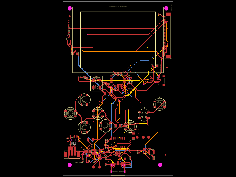
Schematic

import { A_0_5K_AS_50PWBG } from "./imports/A_0_5K_AS_50PWBG"
import { A_4_4_1_7___ } from "./imports/A_4_4_1_7___"
import { A_0402WGF0000TCE } from "./imports/A_0402WGF0000TCE"
import { A_0402WGF1000TCE } from "./imports/A_0402WGF1000TCE"
import { A_0402WGF1001TCE } from "./imports/A_0402WGF1001TCE"
import { A_0402WGF1002TCE } from "./imports/A_0402WGF1002TCE"
import { A_0402WGF3300TCE } from "./imports/A_0402WGF3300TCE"
import { A_0402WGF3301TCE } from "./imports/A_0402WGF3301TCE"
import { A_0402WGF4702TCE } from "./imports/A_0402WGF4702TCE"
import { A_0402WGF5101TCE } from "./imports/A_0402WGF5101TCE"
import { A_1206W4F0000T5E } from "./imports/A_1206W4F0000T5E"
import { AO3400A } from "./imports/AO3400A"
import { B3B_PH_SM4_TB_LF__SN_ } from "./imports/B3B_PH_SM4_TB_LF__SN_"
import { BQ24075RGTR } from "./imports/BQ24075RGTR"
import { CH340C } from "./imports/CH340C"
import { CL05B103KB5NNNC } from "./imports/CL05B103KB5NNNC"
import { CL05B104KO5NNNC } from "./imports/CL05B104KO5NNNC"
import { CL10A106KP8NNNC } from "./imports/CL10A106KP8NNNC"
import { CL10A475KO8NNNC } from "./imports/CL10A475KO8NNNC"
import { CL10B474KA8NNNC } from "./imports/CL10B474KA8NNNC"
import { FNR3015S1R5MT } from "./imports/FNR3015S1R5MT"
import { MSK12C02 } from "./imports/MSK12C02"
import { MSPM0G3507SPTR } from "./imports/MSPM0G3507SPTR"
import { SM04B_SRSS_TB_LF__SN_ } from "./imports/SM04B_SRSS_TB_LF__SN_"
import { SZYY1615RGB_A_4pin } from "./imports/SZYY1615RGB_A_4pin"
import { TS342A2P_WZ } from "./imports/TS342A2P_WZ"
import { TPS61240DRVR } from "./imports/TPS61240DRVR"
import { TPS63031DSKR } from "./imports/TPS63031DSKR"
import { TYPE_C_31_M_12 } from "./imports/TYPE_C_31_M_12"
import { USBLC6_2SC6 } from "./imports/USBLC6_2SC6"
import { XL_1608SYGC_06 } from "./imports/XL_1608SYGC_06"

const cleanComponentSilk = {
  pcbSx: { "& silkscreentext": { visibility: "hidden" as const } },
}

const USB_SCHEMATIC_SHEET = "USB_PROGRAMMING"
const POWER_SCHEMATIC_SHEET = "BATTERY_CHARGER"
const POWER_RAILS_SCHEMATIC_SHEET = "POWER_RAILS"
const GROUND_STAR_SCHEMATIC_SHEET = "GROUND_STAR"
const MCU_SCHEMATIC_SHEET = "MCU_DEBUG"
const DISPLAY_SCHEMATIC_SHEET = "DISPLAY_INTERFACE"
const CONTROLS_SCHEMATIC_SHEET = "GAME_CONTROLS"
const USER_IO_SCHEMATIC_SHEET = "USER_IO"
const schematicSections = {
  usb: "USB_AND_PROGRAMMING",
  powerInput: "BATTERY_AND_CHARGER",
  powerRails: "REGULATED_POWER_RAILS",
  groundStar: "GROUND_DOMAIN_STAR",
  mcu: "MCU",
  display: "DISPLAY",
  controls: "GAME_CONTROLS",
  audio: "AUDIO",
  indicators: "INDICATORS",
} as const

const sheetForSection = {
  [schematicSections.usb]: USB_SCHEMATIC_SHEET,
  [schematicSections.powerInput]: POWER_SCHEMATIC_SHEET,
  [schematicSections.powerRails]: POWER_RAILS_SCHEMATIC_SHEET,
  [schematicSections.groundStar]: GROUND_STAR_SCHEMATIC_SHEET,
  [schematicSections.mcu]: MCU_SCHEMATIC_SHEET,
  [schematicSections.display]: DISPLAY_SCHEMATIC_SHEET,
  [schematicSections.controls]: CONTROLS_SCHEMATIC_SHEET,
  [schematicSections.audio]: USER_IO_SCHEMATIC_SHEET,
  [schematicSections.indicators]: USER_IO_SCHEMATIC_SHEET,
} as const

const schematicSectionStyle = (schSectionName: string) => ({
  ...cleanComponentSilk,
  schSectionName,
  schSheetName: sheetForSection[schSectionName as keyof typeof sheetForSection],
})

const gameControls = [
  { name: "SW_UP", label: "UP", port: "PA2", net: "BTN_UP", x: -22, y: -8, rotation: 90, schX: -8, schY: 6 },
  { name: "SW_DOWN", label: "DOWN", port: "PA3", net: "BTN_DOWN", x: -22, y: -26, rotation: 90, schX: -8, schY: 2 },
  { name: "SW_LEFT", label: "LEFT", port: "PA4", net: "BTN_LEFT", x: -31, y: -17, rotation: 0, schX: -12, schY: 4 },
  { name: "SW_RIGHT", label: "RIGHT", port: "PA5", net: "BTN_RIGHT", x: -13, y: -17, rotation: 0, schX: -4, schY: 4 },
  { name: "SW_A", label: "A", port: "PA6", net: "BTN_A", x: 27.2, y: -11, rotation: 0, schX: 8, schY: 6 },
  { name: "SW_B", label: "B", port: "PA7", net: "BTN_B", x: 17, y: -18, rotation: 0, schX: 4, schY: 2 },
  { name: "SW_START", label: "START", port: "PA12", net: "BTN_START", x: 8, y: -25.5, rotation: 0, schX: 4, schY: -4 },
  { name: "SW_SELECT", label: "SELECT", port: "PA13", net: "BTN_SELECT", x: -8, y: -25, rotation: 0, schX: -4, schY: -4 },
] as const

const displaySignals = [
  { pin: "D_CX_SCL", port: "PB9", net: "DISPLAY_SCK" },
  { pin: "SDI", port: "PB8", net: "DISPLAY_MOSI" },
  { pin: "RESET", port: "PA9", net: "DISPLAY_RESET_N" },
  { pin: "WRX_D_CX", port: "PA8", net: "DISPLAY_DC" },
  { pin: "CSX", port: "PB15", net: "DISPLAY_CS_N" },
  { pin: null, port: "PA16", net: "DISPLAY_BACKLIGHT_PWM" },
] as const

const unusedDisplayPins = [
  "VSYNC", "HSYNC", "DOTCLK", "DE",
  "DB17", "DB16", "DB15", "DB14", "DB13", "DB12", "DB11", "DB10", "DB9",
  "DB8", "DB7", "DB6", "DB5", "DB4", "DB3", "DB2", "DB1", "DB0",
  "SDO", "TE", "TOUCH_SCL", "TOUCH_SDA", "TOUCH_INT", "TOUCH_RESET",
  "SHIELD1", "SHIELD2",
] as const

const testPointFootprint = (
  <footprint>
    <smtpad portHints={["pin1"]} shape="circle" radius="0.9mm" />
    <courtyardcircle pcbX={0} pcbY={0} radius="1.15mm" />
  </footprint>
)

const NamedTrace = ({ name, from, to, schDisplayLabel, pcbRouteHints, routingPhaseIndex }: { name: string, from: string, to: string, schDisplayLabel?: string, pcbRouteHints?: Array<{ x: number, y: number }>, routingPhaseIndex?: number }) => (
  <trace name={name} from={from} to={to} schDisplayLabel={schDisplayLabel} pcbRouteHints={pcbRouteHints} routingPhaseIndex={routingPhaseIndex} />
)

export default function MSPM0G3507GameBoyHandheld() {
  return (
    <board
      title="MSPM0G3507 Game Boy Handheld"
      outline={[
        { x: -36, y: 56 },
        { x: 36, y: 56 },
        { x: 36, y: -56 },
        { x: -36, y: -56 },
      ]}
      layers={4}
      schSheetName={USB_SCHEMATIC_SHEET}
      schY={10}
      schAutoLayoutEnabled
      minViaHoleDiameter="0.3mm"
      minViaPadDiameter="0.45mm"
      minViaEdgeToPadEdgeClearance="0.2mm"
      pcbStyle={{ viaHoleDiameter: "0.3mm", viaPadDiameter: "0.45mm" }}
    >
      <autoroutingphase
        name="GROUND_DOMAIN_ROUTING"
        phaseIndex={-1}
        autorouter="default"
      />
      <schematicsheet
        name={USB_SCHEMATIC_SHEET}
        displayName="1 of 8 — USB-C power and UART programming"
        sheetIndex={1}
        sheetSize="ANSI_B"
      >
        <schematicsection name={schematicSections.usb} />
      </schematicsheet>
      <schematicsheet
        name={POWER_SCHEMATIC_SHEET}
        displayName="2 of 8 — Protected LiPo connector and charger"
        sheetIndex={2}
        sheetSize="A4"
      >
        <schematicsection name={schematicSections.powerInput} />
      </schematicsheet>
      <schematicsheet
        name={POWER_RAILS_SCHEMATIC_SHEET}
        displayName="3 of 8 — Switched 3.3 V and display 5 V rails"
        sheetIndex={3}
        sheetSize="ANSI_B"
      >
        <schematicsection name={schematicSections.powerRails} />
      </schematicsheet>
      <schematicsheet
        name={GROUND_STAR_SCHEMATIC_SHEET}
        displayName="4 of 8 — Ground-domain star links"
        sheetIndex={4}
        sheetSize="A4"
      >
        <schematicsection name={schematicSections.groundStar} />
      </schematicsheet>
      <schematicsheet
        name={MCU_SCHEMATIC_SHEET}
        displayName="5 of 8 — MSPM0G3507 core, boot and debug"
        sheetIndex={5}
        sheetSize="A4"
      >
        <schematicsection name={schematicSections.mcu} />
      </schematicsheet>
      <schematicsheet
        name={DISPLAY_SCHEMATIC_SHEET}
        displayName="6 of 8 — ER-TFT024IPS-3 display interface"
        sheetIndex={6}
        sheetSize="A4"
      >
        <schematicsection name={schematicSections.display} />
      </schematicsheet>
      <schematicsheet
        name={CONTROLS_SCHEMATIC_SHEET}
        displayName="7 of 8 — D-pad and game buttons"
        sheetIndex={7}
        sheetSize="A4"
      >
        <schematicsection name={schematicSections.controls} />
      </schematicsheet>
      <schematicsheet
        name={USER_IO_SCHEMATIC_SHEET}
        displayName="8 of 8 — Audio and indicators"
        sheetIndex={8}
        sheetSize="ANSI_B"
      >
        <schematicsection name={schematicSections.audio} />
        <schematicsection name={schematicSections.indicators} />
      </schematicsheet>

      <TYPE_C_31_M_12
        {...schematicSectionStyle(schematicSections.usb)}
        name="J_USB_C"
        noConnect={["A8", "B8"]}
        obstructsWithinBounds={false}
        pcbX={0}
        pcbY={-52}
        schX={-12.78}
        schY={-4.45}
      />
      <A_1206W4F0000T5E {...schematicSectionStyle(schematicSections.usb)} name="R_USB_DM_JOIN" pcbX={3.0} pcbY={-46.5} obstructsWithinBounds={false} schX={-14.65} schY={-6.69} />
      <A_0402WGF0000TCE {...schematicSectionStyle(schematicSections.usb)} name="R_VBUS_A_LINK" pcbX={-8.0} pcbY={-46.0} pcbRotation={90} obstructsWithinBounds={false} />
      <A_0402WGF0000TCE {...schematicSectionStyle(schematicSections.usb)} name="R_VBUS_B_LINK" pcbX={8.0} pcbY={-46.0} pcbRotation={90} obstructsWithinBounds={false} />
      <USBLC6_2SC6 {...schematicSectionStyle(schematicSections.usb)} name="U_USB_ESD" pcbX={0} pcbY={-43.0} schX={-16.34} schY={-8.43} />
      <CH340C
        {...schematicSectionStyle(schematicSections.usb)}
        name="U_USB_UART"
        noConnect={["NC", "N_OUT", "N_CTS", "N_DSR", "N_RI", "N_DCD", "N_DTR", "N_RTS", "R232"]}
        pcbX={0}
        pcbY={-36.0}
        schX={-9.72}
        schY={-8.95}
      />
      <A_0402WGF5101TCE {...schematicSectionStyle(schematicSections.usb)} name="R_USB_CC1" pcbX={-8.0} pcbY={-50.0} pcbRotation={270} schX={-16.74} schY={-5.25} schRotation={90} />
      <A_0402WGF5101TCE {...schematicSectionStyle(schematicSections.usb)} name="R_USB_CC2" pcbX={8.0} pcbY={-50.0} pcbRotation={270} schX={-12.15} schY={-6.7} schRotation={90} />
      <CL05B104KO5NNNC {...schematicSectionStyle(schematicSections.usb)} name="C_USB_UART" pcbX={7.5} pcbY={-36.0} pcbRotation={90} maxDecouplingTraceLength="30mm" />
      <A_0402WGF1001TCE {...schematicSectionStyle(schematicSections.usb)} name="R_UART_TX" pcbX={8.0} pcbY={-1.0} schX={-13.61} schY={-11.39} />
      <A_0402WGF1001TCE {...schematicSectionStyle(schematicSections.usb)} name="R_UART_RX" pcbX={7.5} pcbY={5.0} schX={-13.65} schY={-10.37} />

      <B3B_PH_SM4_TB_LF__SN_
        {...schematicSectionStyle(schematicSections.powerInput)}
        name="J_BATTERY"
        noConnect={["pin4", "pin5"]}
        pcbX={-30}
        pcbY={-42}
        schX={-12}
        schY={0}
        schHeight={0.6}
      />
      <BQ24075RGTR
        {...schematicSectionStyle(schematicSections.powerInput)}
        name="U_BATTERY_CHARGER"
        noConnect={["N_CHG", "N_PGOOD"]}
        pcbX={-20}
        pcbY={-42}
        schX={-7}
        schY={0}
        schHeight={1.8}
      />
      <CL10A475KO8NNNC {...schematicSectionStyle(schematicSections.powerInput)} name="C_CHARGER_INPUT" pcbX={-20} pcbY={-48} pcbRotation={180} schX={-11} schY={7} schRotation={270} maxDecouplingTraceLength="30mm" />
      <CL10A475KO8NNNC {...schematicSectionStyle(schematicSections.powerInput)} name="C_CHARGER_BATTERY" pcbX={-23.2} pcbY={-47.5} pcbRotation={270} schX={-12} schY={-7} schRotation={270} maxDecouplingTraceLength="30mm" />
      <CL10A106KP8NNNC {...schematicSectionStyle(schematicSections.powerInput)} name="C_CHARGER_SYSTEM" pcbX={-15.5} pcbY={-47.5} pcbRotation={90} schX={-4} schY={-7} schRotation={270} maxDecouplingTraceLength="30mm" />
      <A_0402WGF3301TCE {...schematicSectionStyle(schematicSections.powerInput)} name="R_CHARGE_CURRENT" pcbX={-17} pcbY={-45.5} pcbRotation={270} schX={-8} schY={-7} schRotation={270} />
      <A_0402WGF3301TCE {...schematicSectionStyle(schematicSections.powerInput)} name="R_INPUT_CURRENT_LIMIT" pcbX={-14} pcbY={-45.5} pcbRotation={270} schX={-6} schY={-7} schRotation={270} />
      <A_0402WGF4702TCE {...schematicSectionStyle(schematicSections.powerInput)} name="R_CHARGE_TIMER" pcbX={-17} pcbY={-38} pcbRotation={90} schX={-3} schY={7} schRotation={270} />

      <MSK12C02
        {...schematicSectionStyle(schematicSections.powerRails)}
        name="SW_POWER"
        noConnect={["pin4"]}
        pcbX={-29}
        pcbY={-33.5}
        schX={-0.73}
        schY={7}
      />
      <TPS63031DSKR
        {...schematicSectionStyle(schematicSections.powerRails)}
        name="U_3V3_BUCK_BOOST"
        pcbX={-11.5}
        pcbY={-42}
        schX={3}
        schY={0}
        schHeight={1.2}
      />
      <A_0402WGF0000TCE {...schematicSectionStyle(schematicSections.powerRails)} name="R_POWER_ENABLE_LINK" pcbX={-8.2} pcbY={-44} schX={1} schY={2} schRotation={180} />
      <FNR3015S1R5MT {...schematicSectionStyle(schematicSections.powerRails)} name="L_3V3_BUCK_BOOST" pcbX={-15.6} pcbY={-42} pcbRotation={270} schX={3.73} schY={7} />
      <CL10A106KP8NNNC {...schematicSectionStyle(schematicSections.powerRails)} name="C_3V3_INPUT" pcbX={-11.5} pcbY={-46} pcbRotation={90} schX={-1} schY={-7} schRotation={270} maxDecouplingTraceLength="30mm" />
      <CL05B104KO5NNNC {...schematicSectionStyle(schematicSections.powerRails)} name="C_3V3_INPUT_BYPASS" pcbX={-6} pcbY={-42} pcbRotation={90} schX={1} schY={-9} schRotation={270} maxDecouplingTraceLength="40mm" />
      <CL10A106KP8NNNC {...schematicSectionStyle(schematicSections.powerRails)} name="C_3V3_OUTPUT_A" pcbX={-7.5} pcbY={-38.6} pcbRotation={90} schX={4} schY={-7} schRotation={270} maxDecouplingTraceLength="30mm" />
      <CL10A106KP8NNNC {...schematicSectionStyle(schematicSections.powerRails)} name="C_3V3_OUTPUT_B" pcbX={-7.5} pcbY={-35.0} pcbRotation={90} schX={7} schY={-9} schRotation={270} maxDecouplingTraceLength="30mm" />

      <TPS61240DRVR
        {...schematicSectionStyle(schematicSections.powerRails)}
        name="U_BACKLIGHT_BOOST"
        pcbX={18}
        pcbY={-42}
        schX={9}
        schY={0}
        schHeight={0.8}
      />
      <FNR3015S1R5MT {...schematicSectionStyle(schematicSections.powerRails)} name="L_BACKLIGHT_BOOST" pcbX={21.8} pcbY={-42} pcbRotation={180} schX={10.703} schY={7} schRotation={90} />
      <CL10A475KO8NNNC {...schematicSectionStyle(schematicSections.powerRails)} name="C_BACKLIGHT_BOOST_INPUT" pcbX={13.5} pcbY={-42} pcbRotation={90} schX={9} schY={-7} schRotation={270} maxDecouplingTraceLength="30mm" />
      <CL10A106KP8NNNC {...schematicSectionStyle(schematicSections.powerRails)} name="C_BACKLIGHT_5V_OUTPUT" pcbX={23} pcbY={-46} pcbRotation={90} schX={12} schY={-9} schRotation={270} maxDecouplingTraceLength="30mm" />

      <A_1206W4F0000T5E {...schematicSectionStyle(schematicSections.groundStar)} name="R_GND_USB_LINK" pcbX={10} pcbY={-31.5} pcbRotation={90} schX={-10} schY={0} schRotation={90} />
      <A_1206W4F0000T5E {...schematicSectionStyle(schematicSections.groundStar)} name="R_GND_POWER_LINK" pcbX={-18} pcbY={-34} schX={-6} schY={0} schRotation={90} />
      <A_1206W4F0000T5E {...schematicSectionStyle(schematicSections.groundStar)} name="R_GND_MCU_LINK" pcbX={-7} pcbY={-4} schX={-2} schY={0} schRotation={90} />
      <A_1206W4F0000T5E {...schematicSectionStyle(schematicSections.groundStar)} name="R_GND_CONTROLS_LINK" pcbX={0} pcbY={-25} schX={2} schY={0} schRotation={90} />
      <A_1206W4F0000T5E {...schematicSectionStyle(schematicSections.groundStar)} name="R_GND_DISPLAY_LINK" pcbX={-28} pcbY={22} schX={6} schY={0} schRotation={90} />
      <A_1206W4F0000T5E {...schematicSectionStyle(schematicSections.groundStar)} name="R_GND_IO_LINK" pcbX={24} pcbY={14} schX={10} schY={0} schRotation={90} />

      <MSPM0G3507SPTR
        {...schematicSectionStyle(schematicSections.mcu)}
        name="U_MCU"
        noConnect={["PA0", "PA1", "PA17", "PA21", "PA22", "PA23", "PA24", "PA25", "PA26", "PA27", "PA28", "PA31", "PB6", "PB7", "PB16", "PB17", "PB18", "PB19", "PB20", "PB21"]}
        pcbX={0}
        pcbY={5}
        schX={-12.38}
        schY={-15.98}
        schHeight={5}
      />
      <CL10A106KP8NNNC {...schematicSectionStyle(schematicSections.mcu)} name="C_MCU_BULK" pcbX={-3.0} pcbY={-1.6} schX={-16} schY={-16.66} schRotation={90} />
      <CL05B104KO5NNNC {...schematicSectionStyle(schematicSections.mcu)} name="C_MCU_BYPASS" pcbX={0} pcbY={-1.3} schX={-16.46} schY={-17.82} schRotation={90} maxDecouplingTraceLength="30mm" />
      <CL10B474KA8NNNC {...schematicSectionStyle(schematicSections.mcu)} name="C_MCU_VCORE" pcbX={-6.8} pcbY={2.25} pcbRotation={180} maxDecouplingTraceLength="30mm" />
      <A_0402WGF4702TCE {...schematicSectionStyle(schematicSections.mcu)} name="R_RESET_PULLUP" pcbX={7.0} pcbY={3.0} pcbRotation={90} schX={-16.53} schY={-14.78} schRotation={90} />
      <CL05B103KB5NNNC {...schematicSectionStyle(schematicSections.mcu)} name="C_RESET" pcbX={9.2} pcbY={3.0} pcbRotation={90} schMarginRight={0.6} maxDecouplingTraceLength="30mm" />
      <TS342A2P_WZ {...schematicSectionStyle(schematicSections.mcu)} name="SW_RESET" pcbX={-14} pcbY={0} schX={-16.27} schY={-19.28} schRotation={90} />
      <A_0402WGF1002TCE {...schematicSectionStyle(schematicSections.mcu)} name="R_BOOT_PULLDOWN" pcbX={7.0} pcbY={7.0} pcbRotation={270} />
      <TS342A2P_WZ {...schematicSectionStyle(schematicSections.mcu)} name="SW_BOOT" pcbX={-14} pcbY={5.0} />

      {gameControls.map((control) => (
        <A_4_4_1_7___
          {...schematicSectionStyle(schematicSections.controls)}
          key={control.name}
          name={control.name}
          pcbX={control.x}
          pcbY={control.y}
          pcbRotation={control.rotation}
          schX={control.schX}
          schY={control.schY}
        />
      ))}
      <A_0_5K_AS_50PWBG
        {...schematicSectionStyle(schematicSections.display)}
        name="J_DISPLAY_FPC"
        noConnect={[...unusedDisplayPins]}
        pcbX={32.0}
        pcbY={34.0}
        pcbRotation={90}
        schX={-2.94}
        schY={-4}
      />
      <A_0402WGF0000TCE {...schematicSectionStyle(schematicSections.display)} name="R_DISPLAY_5V_LINK" pcbX={27.0} pcbY={48.0} schX={-7.83} schY={1.34} schRotation={270} />
      <A_0402WGF1000TCE {...schematicSectionStyle(schematicSections.display)} name="R_BACKLIGHT_K1" pcbX={-32.0} pcbY={43.0} pcbRotation={270} schX={-3.99} schY={0.54} schRotation={90} />
      <A_0402WGF1000TCE {...schematicSectionStyle(schematicSections.display)} name="R_BACKLIGHT_K2" pcbX={-32.0} pcbY={40.5} pcbRotation={270} schX={-11.46} schY={-1.6} schRotation={90} />
      <A_0402WGF1000TCE {...schematicSectionStyle(schematicSections.display)} name="R_BACKLIGHT_K3" pcbX={-32.0} pcbY={38.0} pcbRotation={270} schX={-7.18} schY={0.04} schRotation={90} />
      <A_0402WGF1000TCE {...schematicSectionStyle(schematicSections.display)} name="R_BACKLIGHT_K4" pcbX={-32.0} pcbY={35.5} pcbRotation={90} schX={-10.18} schY={-2} schRotation={90} />
      <AO3400A {...schematicSectionStyle(schematicSections.display)} name="U_BACKLIGHT_SWITCH" pcbX={-32.0} pcbY={31.5} pcbRotation={270} schX={-13.51} schY={-1.1} schHeight={0.4} />
      <A_0402WGF1002TCE {...schematicSectionStyle(schematicSections.display)} name="R_BACKLIGHT_GATE_PULLDOWN" pcbX={-32.0} pcbY={27.5} pcbRotation={90} schX={-17.251} schY={0.155} schRotation={270} />

      <SM04B_SRSS_TB_LF__SN_
        {...schematicSectionStyle(schematicSections.audio)}
        name="J_AUDIO_MODULE"
        noConnect={["pin5", "pin6"]}
        pcbX={28.0}
        pcbY={4.5}
        pcbRotation={90}
        schX={-10}
        schY={0}
      />

      <A_0402WGF1001TCE {...schematicSectionStyle(schematicSections.indicators)} name="R_POWER_LED" pcbX={-25.0} pcbY={6.5} schX={-2} schY={3} schRotation={270} />
      <XL_1608SYGC_06 {...schematicSectionStyle(schematicSections.indicators)} name="D_POWER" pcbX={-21.0} pcbY={6.5} schX={-2} schY={0} schRotation={90} />
      <A_0402WGF3300TCE {...schematicSectionStyle(schematicSections.indicators)} name="R_RGB_RED" pcbX={17.0} pcbY={7.5} schX={5} schY={3} schRotation={90} />
      <A_0402WGF3300TCE {...schematicSectionStyle(schematicSections.indicators)} name="R_RGB_GREEN" pcbX={17.0} pcbY={5.0} schX={5} schY={0} schRotation={90} />
      <A_0402WGF3300TCE {...schematicSectionStyle(schematicSections.indicators)} name="R_RGB_BLUE" pcbX={17.0} pcbY={2.5} schX={5} schY={-3} schRotation={270} />
      <SZYY1615RGB_A_4pin {...schematicSectionStyle(schematicSections.indicators)} name="D_USER_RGB" pcbX={22.0} pcbY={5.0} pcbRotation={90} schX={9} schY={3.4} schWidth={1.39} />

      <testpoint name="TP_GND" footprint={testPointFootprint} pcbX={-16} pcbY={-52} schSectionName={schematicSections.mcu} />
      <testpoint name="TP_3V3" footprint={testPointFootprint} pcbX={-12} pcbY={-52} connections={{ pin1: "net.VDD_3V3" }} schSectionName={schematicSections.mcu} />
      <testpoint name="TP_SWDIO" footprint={testPointFootprint} pcbX={12.5} pcbY={-32.5} schSectionName={schematicSections.mcu} />
      <testpoint name="TP_SWCLK" footprint={testPointFootprint} pcbX={16.5} pcbY={-32.5} schSectionName={schematicSections.mcu} />
      <testpoint name="TP_RESET" footprint={testPointFootprint} pcbX={20} pcbY={-32.5} connections={{ pin1: "net.MCU_RESET_N" }} schSectionName={schematicSections.mcu} />

      <hole name="H1" pcbX={-31.5} pcbY={51.5} diameter="2.7mm" />
      <hole name="H2" pcbX={31.5} pcbY={51.5} diameter="2.7mm" />
      <hole name="H3" pcbX={-31.5} pcbY={-50.5} diameter="2.7mm" />
      <hole name="H4" pcbX={27.5} pcbY={-50.5} diameter="2.7mm" />
      <fiducial name="FID1" pcbX={-31.5} pcbY={46.5} padDiameter="1mm" soldermaskPullback="1mm" />
      <fiducial name="FID2" pcbX={32.0} pcbY={13.0} padDiameter="1mm" soldermaskPullback="1mm" />
      <fiducial name="FID3" pcbX={31.0} pcbY={-44.0} padDiameter="1mm" soldermaskPullback="1mm" />

      <silkscreenrect pcbX={0} pcbY={31.0} width="59.26mm" height="42.72mm" strokeWidth="0.25mm" />
      <silkscreenrect pcbX={0} pcbY={31.0} width="48.96mm" height="36.72mm" strokeWidth="0.35mm" />
      <silkscreentext text="ER-TFT024IPS-3 / ST7789 / 320x240" pcbX={0} pcbY={52.9} fontSize="0.65mm" />
      <silkscreentext text="MSPM0 POCKET" pcbX={0} pcbY={8.2} fontSize="1.0mm" />
      <silkscreentext text="UP" pcbX={-22} pcbY={-3.8} fontSize="0.8mm" />
      <silkscreentext text="DOWN" pcbX={-22} pcbY={-30.2} fontSize="0.8mm" />
      <silkscreentext text="LEFT" pcbX={-31} pcbY={-21.2} fontSize="0.8mm" />
      <silkscreentext text="RIGHT" pcbX={-13} pcbY={-21.2} fontSize="0.8mm" />
      <silkscreentext text="A" pcbX={27.2} pcbY={-6.5} fontSize="1.2mm" />
      <silkscreentext text="B" pcbX={17} pcbY={-13.5} fontSize="1.2mm" />
      <silkscreentext text="START" pcbX={8} pcbY={-29.7} fontSize="0.7mm" />
      <silkscreentext text="SELECT" pcbX={-8} pcbY={-29.2} fontSize="0.7mm" />
      <silkscreenrect pcbX={-14} pcbY={2.5} width="8mm" height="10mm" strokeWidth="0.25mm" />
      <silkscreentext text="RESET" pcbX={-14} pcbY={-2.4} fontSize="0.5mm" />
      <silkscreentext text="BOOT" pcbX={-14} pcbY={7.2} fontSize="0.5mm" />
      <silkscreentext text="SERVICE PINHOLES" pcbX={-14} pcbY={8.2} fontSize="0.45mm" />
      <silkscreentext text="DISPLAY FPC PIN 1" pcbX={34.7} pcbY={52.0} pcbRotation={90} fontSize="0.45mm" />
      <silkscreentext text="AUDIO: G 3V3 PWM EN" pcbX={28.0} pcbY={12.0} pcbRotation={90} fontSize="0.55mm" />
      <silkscreentext text="USB-C POWER + PROGRAM" pcbX={0} pcbY={-55.0} fontSize="0.55mm" />
      <silkscreentext text="BAT 3:-  2:NTC  1:+" pcbX={-29.5} pcbY={-37.2} fontSize="0.45mm" />
      <silkscreentext text="PROTECTED 1S LiPo ONLY" pcbX={-25.5} pcbY={-48.8} fontSize="0.45mm" />
      <silkscreentext text="OFF" pcbX={-33.2} pcbY={-33.4} fontSize="0.5mm" />
      <silkscreentext text="ON" pcbX={-24.4} pcbY={-33.4} fontSize="0.5mm" />
      <silkscreencircle pcbX={-22} pcbY={-8} radius="4mm" strokeWidth="0.2mm" />
      <silkscreencircle pcbX={-22} pcbY={-26} radius="4mm" strokeWidth="0.2mm" />
      <silkscreencircle pcbX={-31} pcbY={-17} radius="4mm" strokeWidth="0.2mm" />
      <silkscreencircle pcbX={-13} pcbY={-17} radius="4mm" strokeWidth="0.2mm" />
      <silkscreencircle pcbX={27.2} pcbY={-11} radius="4mm" strokeWidth="0.2mm" />
      <silkscreencircle pcbX={17} pcbY={-18} radius="4mm" strokeWidth="0.2mm" />
      <silkscreencircle pcbX={8} pcbY={-25.5} radius="4mm" strokeWidth="0.2mm" />
      <silkscreencircle pcbX={-8} pcbY={-25} radius="4mm" strokeWidth="0.2mm" />

      <trace name="USB_VBUS_A_IN" from="J_USB_C.A4B9" to="R_VBUS_A_LINK.pin1" thickness="0.5mm" pcbRouteHints={[{ x: -4, y: -48 }, { x: -7, y: -48 }]} />
      <trace name="GROUND_TEST_POINT" from="TP_GND.pin1" to="net.GND_MCU" routingPhaseIndex={-1} />
      <trace name="USB_VBUS_B_IN" from="J_USB_C.B4A9" to="R_VBUS_B_LINK.pin1" thickness="0.5mm" />
      <trace from="R_VBUS_A_LINK.pin2" to="net.VBUS_5V" thickness="0.5mm" />
      <trace from="R_VBUS_B_LINK.pin2" to="net.VBUS_5V" thickness="0.5mm" />
      <trace from="J_USB_C.A1B12" to="net.GND_USB" thickness="0.5mm" routingPhaseIndex={-1} />
      <trace from="J_USB_C.B1A12" to="net.GND_USB" thickness="0.5mm" routingPhaseIndex={-1} />
      <trace from="J_USB_C.EH1" to="net.GND_USB" thickness="0.5mm" routingPhaseIndex={-1} />
      <trace from="J_USB_C.EH2" to="net.GND_USB" thickness="0.5mm" routingPhaseIndex={-1} />
      <trace from="J_USB_C.EH3" to="net.GND_USB" thickness="0.5mm" routingPhaseIndex={-1} />
      <trace from="J_USB_C.EH4" to="net.GND_USB" thickness="0.5mm" routingPhaseIndex={-1} />
      <trace
        name="USB_CC1"
        from="J_USB_C.A5"
        to="R_USB_CC1.pin1"
        thickness="0.15mm"
        pcbPath={[
          { x: -1.25, y: 3.8 },
          { x: -6.0, y: 3.8 },
        ]}
      />
      <trace from="R_USB_CC1.pin2" to="net.GND_USB" routingPhaseIndex={-1} />
      <trace
        name="USB_CC2"
        from="J_USB_C.B5"
        to="R_USB_CC2.pin1"
        thickness="0.15mm"
        pcbPath={[
          { x: 1.75, y: 3.2 },
          { x: 8.0, y: 3.2 },
        ]}
      />
      <trace from="R_USB_CC2.pin2" to="net.GND_USB" routingPhaseIndex={-1} />
      <trace
        name="USB_DP_FLIP_A"
        from="J_USB_C.A6"
        to="U_USB_ESD.pin1"
        thickness="0.15mm"
        pcbPath={[
          { x: -0.25, y: 3.3 },
          { x: -0.95, y: 7.3 },
        ]}
      />
      <trace name="USB_DP_FLIP_B" from="J_USB_C.B6" to="U_USB_ESD.pin1" thickness="0.15mm" maxViaCount={2} />
      <trace
        name="USB_DM_FLIP_A"
        from="J_USB_C.A7"
        to="R_USB_DM_JOIN.pin1"
        thickness="0.15mm"
        pcbPath={[
          { x: 0.25, y: 3.8 },
          { x: 1.52, y: 3.8 },
        ]}
      />
      <trace
        name="USB_DM_FLIP_B"
        from="J_USB_C.B7"
        to="R_USB_DM_JOIN.pin2"
        thickness="0.15mm"
        pcbPath={[
          { x: -0.75, y: 2.6 },
          { x: -0.75, y: 2.6, via: true, fromLayer: "top", toLayer: "bottom" },
          { x: -0.75, y: 2.6 },
          { x: 4.48, y: 5.0 },
          { x: 4.48, y: 5.4 },
          { x: 4.48, y: 5.4, via: true, fromLayer: "bottom", toLayer: "top" },
          { x: 4.48, y: 5.4 },
        ]}
      />
      <trace name="USB_DM_TO_ESD" from="R_USB_DM_JOIN.pin1" to="U_USB_ESD.pin3" thickness="0.15mm" maxViaCount={2} routingPhaseIndex={1} />
      <trace
        name="USB_DP_PROTECTED"
        from="U_USB_ESD.pin6"
        to="U_USB_UART.D_POS"
        thickness="0.15mm"
        maxViaCount={0}
        pcbPath={[
          { x: -0.95, y: 1.15 },
          { x: 0.635, y: 4.1275 },
        ]}
      />
      <trace
        name="USB_DM_PROTECTED"
        from="U_USB_ESD.pin4"
        to="U_USB_UART.D_NEG"
        thickness="0.15mm"
        maxViaCount={0}
        pcbPath={[
          { x: 0.95, y: 1.15 },
          { x: 1.905, y: 4.1275 },
        ]}
      />
      <trace from="U_USB_ESD.GND" to="net.GND_USB" routingPhaseIndex={-1} />
      <trace from="U_USB_ESD.VBUS" to="net.VBUS_5V" />

      <trace from="U_USB_UART.GND" to="net.GND_USB" thickness="0.35mm" routingPhaseIndex={-1} />
      <trace from="U_USB_UART.VCC" to="net.VDD_3V3" thickness="0.35mm" />
      <trace from="U_USB_UART.V3" to="net.VDD_3V3" thickness="0.35mm" />
      <trace from="C_USB_UART.pin1" to="net.VDD_3V3" />
      <trace from="C_USB_UART.pin2" to="net.GND_USB" routingPhaseIndex={-1} />
      <trace name="USB_UART_TO_MCU_RX" from="U_USB_UART.TXD" to="R_UART_TX.pin1" />
      <trace from="R_UART_TX.pin2" to="net.UART_RX" />
      <trace
        name="MCU_TX_TO_USB_UART"
        from="U_MCU.PA10"
        to="R_UART_RX.pin1"
        schDisplayLabel="UART_TX"
      />
      <trace name="USB_UART_RXD_INPUT" from="R_UART_RX.pin2" to="U_USB_UART.RXD" />

      <trace from="J_BATTERY.pin1" to="net.BATTERY_POSITIVE" thickness="0.5mm" />
      <trace from="J_BATTERY.pin2" to="net.BATTERY_NTC" />
      <trace from="J_BATTERY.pin3" to="net.GND_POWER" thickness="0.5mm" routingPhaseIndex={-1} />

      <trace from="U_BATTERY_CHARGER.IN" to="net.VBUS_5V" thickness="0.5mm" />
      <trace from="U_BATTERY_CHARGER.BAT1" to="net.BATTERY_POSITIVE" thickness="0.5mm" />
      <trace from="U_BATTERY_CHARGER.BAT2" to="net.BATTERY_POSITIVE" thickness="0.5mm" />
      <trace from="U_BATTERY_CHARGER.TS" to="net.BATTERY_NTC" />
      <trace from="U_BATTERY_CHARGER.OUT1" to="net.VSYS_BAT" thickness="0.5mm" />
      <trace from="U_BATTERY_CHARGER.OUT2" to="net.VSYS_BAT" thickness="0.5mm" />
      <trace from="U_BATTERY_CHARGER.EN1" to="net.VSYS_BAT" />
      <trace from="U_BATTERY_CHARGER.EN2" to="net.GND_POWER" routingPhaseIndex={-1} />
      <trace from="U_BATTERY_CHARGER.N_CE" to="net.GND_POWER" routingPhaseIndex={-1} />
      <trace from="U_BATTERY_CHARGER.SYSOFF" to="net.GND_POWER" routingPhaseIndex={-1} />
      <trace from="U_BATTERY_CHARGER.VSS" to="net.GND_POWER" thickness="0.4mm" routingPhaseIndex={-1} />
      <trace from="U_BATTERY_CHARGER.EP" to="net.GND_POWER" thickness="0.5mm" routingPhaseIndex={-1} />
      <trace name="CHARGE_CURRENT_PROGRAM" from="U_BATTERY_CHARGER.ISET" to="R_CHARGE_CURRENT.pin1" />
      <trace from="R_CHARGE_CURRENT.pin2" to="net.GND_POWER" routingPhaseIndex={-1} />
      <trace name="INPUT_CURRENT_PROGRAM" from="U_BATTERY_CHARGER.ILIM" to="R_INPUT_CURRENT_LIMIT.pin1" />
      <trace from="R_INPUT_CURRENT_LIMIT.pin2" to="net.GND_POWER" routingPhaseIndex={-1} />
      <trace name="CHARGE_TIMER_PROGRAM" from="U_BATTERY_CHARGER.TMR" to="R_CHARGE_TIMER.pin1" />
      <trace from="R_CHARGE_TIMER.pin2" to="net.GND_POWER" routingPhaseIndex={-1} />
      <trace from="C_CHARGER_INPUT.pin1" to="net.VBUS_5V" thickness="0.4mm" />
      <trace from="C_CHARGER_INPUT.pin2" to="net.GND_POWER" thickness="0.4mm" routingPhaseIndex={-1} />
      <trace from="C_CHARGER_BATTERY.pin1" to="net.BATTERY_POSITIVE" thickness="0.4mm" />
      <trace from="C_CHARGER_BATTERY.pin2" to="net.GND_POWER" thickness="0.4mm" routingPhaseIndex={-1} />
      <trace from="C_CHARGER_SYSTEM.pin1" to="net.VSYS_BAT" thickness="0.4mm" />
      <trace from="C_CHARGER_SYSTEM.pin2" to="net.GND_POWER" thickness="0.4mm" routingPhaseIndex={-1} />

      <trace from="SW_POWER.pin1" to="net.GND_POWER" routingPhaseIndex={-1} />
      <trace from="SW_POWER.pin2" to="net.POWER_ENABLE" routingPhaseIndex={0} />
      <trace from="SW_POWER.pin3" to="net.VSYS_BAT" />

      <trace from="U_3V3_BUCK_BOOST.VIN" to="net.VSYS_BAT" thickness="0.5mm" />
      <trace from="U_3V3_BUCK_BOOST.VINA" to="net.VSYS_BAT" />
      <trace from="R_POWER_ENABLE_LINK.pin2" to="net.POWER_ENABLE" routingPhaseIndex={0} />
      <trace name="REGULATOR_ENABLE_LOCAL" from="R_POWER_ENABLE_LINK.pin1" to="U_3V3_BUCK_BOOST.EN" maxLength="5mm" maxViaCount={0} routingPhaseIndex={0} />
      <trace from="U_3V3_BUCK_BOOST.pin7" to="net.GND_POWER" routingPhaseIndex={-1} />
      <trace from="U_3V3_BUCK_BOOST.PGND" to="net.GND_POWER" thickness="0.5mm" routingPhaseIndex={-1} />
      <trace from="U_3V3_BUCK_BOOST.GND" to="net.GND_POWER" thickness="0.4mm" routingPhaseIndex={-1} />
      <trace from="U_3V3_BUCK_BOOST.EP" to="net.GND_POWER" thickness="0.5mm" routingPhaseIndex={-1} />
      <trace name="REGULATOR_3V3_SWITCH_NODE_A" from="U_3V3_BUCK_BOOST.L1" to="L_3V3_BUCK_BOOST.pin1" pcbStraightLine />
      <trace name="REGULATOR_3V3_SWITCH_NODE_B" from="L_3V3_BUCK_BOOST.pin2" to="U_3V3_BUCK_BOOST.L2" pcbStraightLine />
      <trace from="U_3V3_BUCK_BOOST.VOUT" to="net.VDD_3V3" thickness="0.5mm" />
      <trace from="U_3V3_BUCK_BOOST.FB" to="net.VDD_3V3" />
      <trace from="C_3V3_INPUT.pin1" to="net.VSYS_BAT" thickness="0.4mm" />
      <trace from="C_3V3_INPUT.pin2" to="net.GND_POWER" thickness="0.4mm" routingPhaseIndex={-1} />
      <trace from="C_3V3_INPUT_BYPASS.pin1" to="net.VSYS_BAT" />
      <trace from="C_3V3_INPUT_BYPASS.pin2" to="net.GND_POWER" routingPhaseIndex={-1} />
      <trace from="C_3V3_OUTPUT_A.pin1" to="net.VDD_3V3" thickness="0.4mm" />
      <trace from="C_3V3_OUTPUT_A.pin2" to="net.GND_POWER" thickness="0.4mm" routingPhaseIndex={-1} />
      <trace from="C_3V3_OUTPUT_B.pin1" to="net.VDD_3V3" thickness="0.4mm" />
      <trace from="C_3V3_OUTPUT_B.pin2" to="net.GND_POWER" thickness="0.4mm" routingPhaseIndex={-1} />

      <trace from="U_BACKLIGHT_BOOST.VIN" to="net.VSYS_BAT" thickness="0.4mm" />
      <trace from="U_BACKLIGHT_BOOST.EN" to="net.POWER_ENABLE" routingPhaseIndex={0} />
      <trace from="U_BACKLIGHT_BOOST.GND" to="net.GND_POWER" thickness="0.4mm" routingPhaseIndex={-1} />
      <trace from="U_BACKLIGHT_BOOST.PP" to="net.GND_POWER" thickness="0.5mm" routingPhaseIndex={-1} />
      <trace name="BACKLIGHT_5V_SWITCH_NODE" from="U_BACKLIGHT_BOOST.L" to="L_BACKLIGHT_BOOST.pin1" pcbStraightLine />
      <trace from="L_BACKLIGHT_BOOST.pin2" to="net.VSYS_BAT" thickness="0.4mm" />
      <trace from="U_BACKLIGHT_BOOST.VOUT" to="net.DISPLAY_5V" thickness="0.4mm" />
      <trace from="U_BACKLIGHT_BOOST.FB" to="net.DISPLAY_5V" />
      <trace from="C_BACKLIGHT_BOOST_INPUT.pin1" to="net.VSYS_BAT" thickness="0.4mm" />
      <trace from="C_BACKLIGHT_BOOST_INPUT.pin2" to="net.GND_POWER" thickness="0.4mm" routingPhaseIndex={-1} />
      <trace from="C_BACKLIGHT_5V_OUTPUT.pin1" to="net.DISPLAY_5V" thickness="0.4mm" />
      <trace from="C_BACKLIGHT_5V_OUTPUT.pin2" to="net.GND_POWER" thickness="0.4mm" routingPhaseIndex={-1} />

      <trace name="GROUND_USB_DOMAIN" from="R_GND_USB_LINK.pin1" to="net.GND_USB" thickness="0.5mm" routingPhaseIndex={-1} />
      <trace from="R_GND_USB_LINK.pin2" to="net.GND" thickness="0.5mm" routingPhaseIndex={-1} />
      <trace name="GROUND_POWER_DOMAIN" from="R_GND_POWER_LINK.pin1" to="net.GND_POWER" thickness="0.5mm" routingPhaseIndex={-1} />
      <trace from="R_GND_POWER_LINK.pin2" to="net.GND" thickness="0.5mm" routingPhaseIndex={-1} />
      <trace name="GROUND_MCU_DOMAIN" from="R_GND_MCU_LINK.pin1" to="net.GND_MCU" thickness="0.5mm" routingPhaseIndex={-1} />
      <trace from="R_GND_MCU_LINK.pin2" to="net.GND" thickness="0.5mm" routingPhaseIndex={-1} />
      <trace name="GROUND_CONTROLS_DOMAIN" from="R_GND_CONTROLS_LINK.pin1" to="net.GND_CONTROLS" thickness="0.5mm" routingPhaseIndex={-1} />
      <trace from="R_GND_CONTROLS_LINK.pin2" to="net.GND" thickness="0.5mm" routingPhaseIndex={-1} />
      <trace name="GROUND_DISPLAY_DOMAIN" from="R_GND_DISPLAY_LINK.pin1" to="net.GND_DISPLAY" thickness="0.5mm" routingPhaseIndex={-1} />
      <trace from="R_GND_DISPLAY_LINK.pin2" to="net.GND" thickness="0.5mm" routingPhaseIndex={-1} />
      <trace name="GROUND_IO_DOMAIN" from="R_GND_IO_LINK.pin1" to="net.GND_IO" thickness="0.5mm" routingPhaseIndex={-1} />
      <trace from="R_GND_IO_LINK.pin2" to="net.GND" thickness="0.5mm" routingPhaseIndex={-1} />

      <trace from="U_MCU.VDD" to="net.VDD_3V3" thickness="0.4mm" />
      <trace from="U_MCU.VSS" to="net.GND_MCU" thickness="0.4mm" routingPhaseIndex={-1} />
      <trace from="C_MCU_BULK.pin1" to="net.VDD_3V3" thickness="0.35mm" />
      <trace from="C_MCU_BULK.pin2" to="net.GND_MCU" thickness="0.35mm" routingPhaseIndex={-1} />
      <trace name="MCU_VDD_LOCAL_BYPASS" from="C_MCU_BYPASS.pin1" to="U_MCU.VDD" pcbStraightLine />
      <trace name="MCU_GND_LOCAL_BYPASS" from="C_MCU_BYPASS.pin2" to="U_MCU.VSS" pcbStraightLine />
      <trace name="VCORE_DECOUPLE" from="U_MCU.VCORE" to="C_MCU_VCORE.pin1" maxLength="4mm" maxViaCount={0} routingPhaseIndex={0} />
      <trace from="C_MCU_VCORE.pin2" to="net.GND_MCU" routingPhaseIndex={-1} />
      <trace from="U_MCU.NRST" to="net.MCU_RESET_N" />
      <trace from="R_RESET_PULLUP.pin1" to="net.VDD_3V3" />
      <trace from="R_RESET_PULLUP.pin2" to="net.MCU_RESET_N" />
      <trace from="C_RESET.pin1" to="net.MCU_RESET_N" />
      <trace from="C_RESET.pin2" to="net.GND_MCU" routingPhaseIndex={-1} />
      <trace from="SW_RESET.pin1" to="net.MCU_RESET_N" />
      <trace from="SW_RESET.pin2" to="net.GND_MCU" routingPhaseIndex={-1} />
      <trace from="R_BOOT_PULLDOWN.pin1" to="net.BOOT_INVOKE" />
      <trace from="R_BOOT_PULLDOWN.pin2" to="net.GND_MCU" routingPhaseIndex={-1} />
      <trace from="SW_BOOT.pin1" to="net.BOOT_INVOKE" />
      <trace from="SW_BOOT.pin2" to="net.VDD_3V3" />
      <trace from="U_MCU.PA11" to="net.UART_RX" />
      <trace from="U_MCU.PA18" to="net.BOOT_INVOKE" />
      <trace
        name="SWDIO_SERVICE"
        from="U_MCU.PA19"
        to="TP_SWDIO.pin1"
        schDisplayLabel="SWDIO"
      />
      <trace
        name="SWCLK_SERVICE"
        from="U_MCU.PA20"
        to="TP_SWCLK.pin1"
        schDisplayLabel="SWCLK"
      />

      {gameControls.map((control) => (
        <NamedTrace
          key={`mcu-${control.name}`}
          name={`MCU_${control.net}`}
          from={`U_MCU.${control.port}`}
          to={control.name === "SW_UP" || control.name === "SW_LEFT" || control.name === "SW_START" ? `${control.name}.pin1` : `net.${control.net}`}
          schDisplayLabel={control.name === "SW_UP" || control.name === "SW_LEFT" || control.name === "SW_START" ? control.net : undefined}
          pcbRouteHints={control.name === "SW_UP" ? [
            { x: 0.75, y: -0.5 },
            { x: 2.5, y: -3.0 },
            { x: -19.0, y: -3.0 },
          ] : undefined}
        />
      ))}
      {gameControls.filter((control) => control.name !== "SW_UP" && control.name !== "SW_LEFT" && control.name !== "SW_START").map((control) => (
        <NamedTrace key={`switch-${control.name}`} name={`${control.name}_SIGNAL`} from={`${control.name}.pin1`} to={`net.${control.net}`} />
      ))}
      {gameControls.map((control) => (
        <NamedTrace key={`ground-${control.name}`} name={`${control.name}_GROUND`} from={`${control.name}.pin2`} to="net.GND_CONTROLS" schDisplayLabel="GND_CONTROLS" routingPhaseIndex={-1} />
      ))}

      <trace
        name="DISPLAY_BACKLIGHT_5V"
        from="J_DISPLAY_FPC.LEDA"
        to="R_DISPLAY_5V_LINK.pin2"
        thickness="0.35mm"
        maxViaCount={2}
      />
      <trace from="R_DISPLAY_5V_LINK.pin1" to="net.DISPLAY_5V" thickness="0.35mm" />
      <trace from="J_DISPLAY_FPC.IM0" to="net.GND_DISPLAY" routingPhaseIndex={-1} />
      <trace from="J_DISPLAY_FPC.IM1" to="net.VDD_3V3" />
      <trace from="J_DISPLAY_FPC.IM2" to="net.VDD_3V3" />
      <trace from="J_DISPLAY_FPC.IM3" to="net.GND_DISPLAY" routingPhaseIndex={-1} />
      <trace from="J_DISPLAY_FPC.RD" to="net.VDD_3V3" />
      <trace from="J_DISPLAY_FPC.VDDI1" to="net.VDD_3V3" thickness="0.35mm" />
      <trace from="J_DISPLAY_FPC.VDDI2" to="net.VDD_3V3" thickness="0.35mm" />
      <trace from="J_DISPLAY_FPC.VCI" to="net.VDD_3V3" thickness="0.35mm" />
      <trace from="J_DISPLAY_FPC.GND1" to="net.GND_DISPLAY" thickness="0.35mm" routingPhaseIndex={-1} />
      <trace from="J_DISPLAY_FPC.GND2" to="net.GND_DISPLAY" thickness="0.35mm" routingPhaseIndex={-1} />
      <trace from="J_DISPLAY_FPC.GND3" to="net.GND_DISPLAY" thickness="0.35mm" routingPhaseIndex={-1} />
      <trace from="J_DISPLAY_FPC.GND4" to="net.GND_DISPLAY" thickness="0.35mm" routingPhaseIndex={-1} />
      {displaySignals.map((signal) => (
        <NamedTrace key={`display-mcu-${signal.net}`} name={`MCU_${signal.net}`} from={`U_MCU.${signal.port}`} to={`net.${signal.net}`} />
      ))}
      {displaySignals.filter((signal) => signal.pin !== null).map((signal) => (
        <NamedTrace key={`display-connector-${signal.net}`} name={`DISPLAY_${signal.net}`} from={`J_DISPLAY_FPC.${signal.pin}`} to={`net.${signal.net}`} />
      ))}
      <trace name="BACKLIGHT_K1_CURRENT_LIMIT" from="J_DISPLAY_FPC.LEDK1" to="R_BACKLIGHT_K1.pin1" />
      <trace name="BACKLIGHT_K2_CURRENT_LIMIT" from="J_DISPLAY_FPC.LEDK2" to="R_BACKLIGHT_K2.pin1" />
      <trace name="BACKLIGHT_K3_CURRENT_LIMIT" from="J_DISPLAY_FPC.LEDK3" to="R_BACKLIGHT_K3.pin1" />
      <trace name="BACKLIGHT_K4_CURRENT_LIMIT" from="J_DISPLAY_FPC.LEDK4" to="R_BACKLIGHT_K4.pin1" />
      <trace from="R_BACKLIGHT_K1.pin2" to="net.DISPLAY_BACKLIGHT_SINK" />
      <trace from="R_BACKLIGHT_K2.pin2" to="net.DISPLAY_BACKLIGHT_SINK" />
      <trace from="R_BACKLIGHT_K3.pin2" to="net.DISPLAY_BACKLIGHT_SINK" />
      <trace from="R_BACKLIGHT_K4.pin2" to="net.DISPLAY_BACKLIGHT_SINK" />
      <trace from="U_BACKLIGHT_SWITCH.D" to="net.DISPLAY_BACKLIGHT_SINK" thickness="0.35mm" />
      <trace from="U_BACKLIGHT_SWITCH.S" to="net.GND_DISPLAY" thickness="0.35mm" routingPhaseIndex={-1} />
      <trace from="U_BACKLIGHT_SWITCH.G" to="net.DISPLAY_BACKLIGHT_PWM" />
      <trace from="R_BACKLIGHT_GATE_PULLDOWN.pin1" to="net.DISPLAY_BACKLIGHT_PWM" />
      <trace from="R_BACKLIGHT_GATE_PULLDOWN.pin2" to="net.GND_DISPLAY" routingPhaseIndex={-1} />

      <trace from="J_AUDIO_MODULE.pin1" to="net.GND_IO" routingPhaseIndex={-1} />
      <trace from="J_AUDIO_MODULE.pin2" to="net.VDD_3V3" thickness="0.35mm" />
      <trace from="J_AUDIO_MODULE.pin3" to="net.AUDIO_PWM" />
      <trace from="J_AUDIO_MODULE.pin4" to="net.AUDIO_ENABLE" />
      <trace from="U_MCU.PA14" to="net.AUDIO_PWM" />
      <trace from="U_MCU.PA15" to="net.AUDIO_ENABLE" />

      <trace from="net.VDD_3V3" to="R_POWER_LED.pin1" />
      <trace name="POWER_LED_ANODE" from="R_POWER_LED.pin2" to="D_POWER.anode" />
      <trace from="D_POWER.cathode" to="net.GND_IO" routingPhaseIndex={-1} />
      <trace from="U_MCU.PB2" to="net.RGB_RED" />
      <trace from="net.RGB_RED" to="R_RGB_RED.pin1" />
      <trace name="RGB_RED_ANODE" from="R_RGB_RED.pin2" to="D_USER_RGB.pin1" />
      <trace from="U_MCU.PB3" to="net.RGB_GREEN" />
      <trace from="net.RGB_GREEN" to="R_RGB_GREEN.pin1" />
      <trace name="RGB_GREEN_ANODE" from="R_RGB_GREEN.pin2" to="D_USER_RGB.pin2" />
      <trace from="U_MCU.PB14" to="net.RGB_BLUE" />
      <trace from="net.RGB_BLUE" to="R_RGB_BLUE.pin1" />
      <trace name="RGB_BLUE_ANODE" from="R_RGB_BLUE.pin2" to="D_USER_RGB.pin3" />
      <trace from="D_USER_RGB.pin4" to="net.GND_IO" routingPhaseIndex={-1} />

    </board>
  )
}
Related Packages
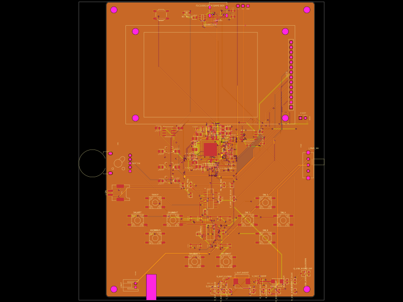 More from this authorShiboSoftwareDev/f1c100s-linux-gameboyRestores PCB assembly metadata by assigning part numbers, managing 3D CAD models and orientations, removing test-point bodies, and validating top-side SMT solder-paste features.
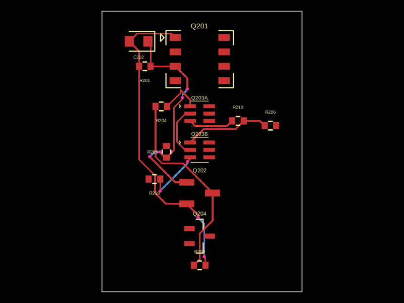 Similar packageastrimid/ec_driven_dc_isolationThis code models a power control circuit featuring NPN and P-channel MOSFETs, resistors, and capacitors, including a dual N-channel MOSFET package, to manage power paths and switching functions on a hardware PCB.
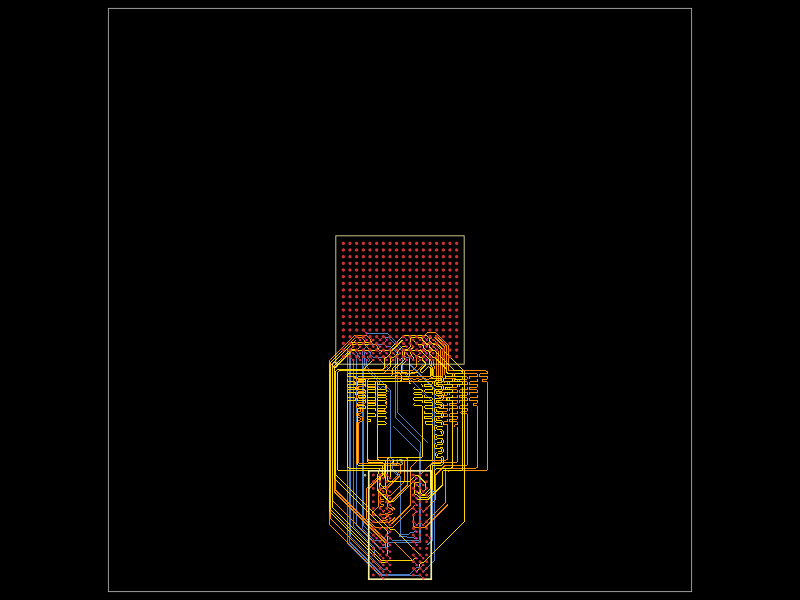 Discover something newseveibar/am3352-ram-dogbone-and-single-layer-route-testAM3352BZCZ100 processor connected to a W631GG6MB-12 DDR3 memory chip through a routed, length-matched 16-bit DDR interface with clock/data-strobe pairs and control/address signals.