ShiboSoftwareDev/lp-msp430fr2476
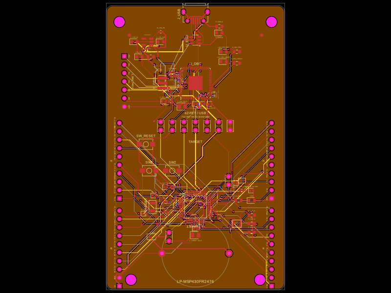
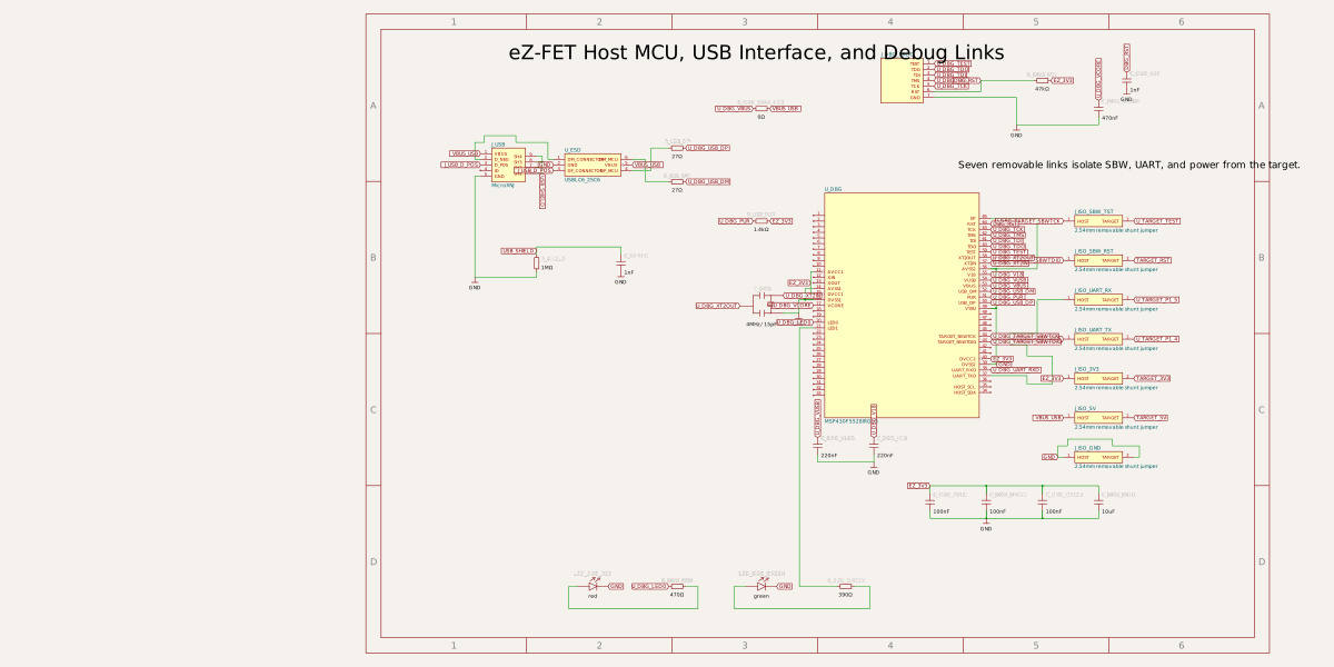
This design implements a microcontroller-based development board featuring an MSP430FR2476 target MCU with associated power regulation, USB host interface with ESD protection, multiple headers for peripherals and BoosterPacks, and integrated status LEDs and sensors.
- Version
- 1.0.0
- License
- unset
- Stars
- 0
index.circuit.tsx
PCB
Schematic
import { CSTCR4M00G53_R0 } from "./imports/CSTCR4M00G53_R0"
import { MicroXNJ } from "./imports/MicroXNJ"
import { MSP430F5528IRGCR } from "./imports/MSP430F5528IRGCR"
import { MSP430FR2476TPT } from "./imports/MSP430FR2476TPT"
import { SC_32S32_768kHz20PPM12_5pF } from "./imports/SC_32S32_768kHz20PPM12_5pF"
import { TS342A2P_WZ } from "./imports/TS342A2P_WZ"
import { USBLC6_2SC6 } from "./imports/USBLC6_2SC6"

// TI's reference is four sheets: eZ-FET host, power, target/headers, and UI.
// These coordinates only control schematic presentation.
const onSheet = <const T extends Record<string, unknown>>(
  schSheetName: string,
  placement: T,
) => ({ schSheetName, ...placement })

const SCH = {
  J_USB: onSheet("DEBUG", { schX: -11, schY: 6 }),
  U_ESD: onSheet("DEBUG", { schX: -8, schY: 6, schRotation: 180 }),
  R_USB_DM: onSheet("DEBUG", { schX: -5, schY: 5.4, schOrientation: "horizontal" }),
  R_USB_DP: onSheet("DEBUG", { schX: -5, schY: 6.6, schOrientation: "horizontal" }),
  R_USB_PUR: onSheet("DEBUG", { schX: -2, schY: 4, schOrientation: "horizontal" }),
  R_DBG_VBUS_LINK: onSheet("DEBUG", { schX: -2, schY: 8, schOrientation: "horizontal" }),
  R_SHIELD: onSheet("DEBUG", { schX: -10, schY: 2.5, schOrientation: "vertical" }),
  C_SHIELD: onSheet("DEBUG", { schX: -7, schY: 2.5, schOrientation: "vertical" }),
  U_LDO: onSheet("POWER", { schX: -2, schY: 2 }),
  C_LDO_IN: onSheet("POWER", { schX: -8, schY: -2, schOrientation: "vertical" }),
  C_LDO_OUT: onSheet("POWER", { schX: 4, schY: -2, schOrientation: "vertical" }),
  R_LDO_EN: onSheet("POWER", { schX: -7, schY: 3, schOrientation: "horizontal" }),
  R_LED_PWR: onSheet("POWER", { schX: 8, schY: 0, schOrientation: "vertical" }),
  LED_PWR: onSheet("POWER", { schX: 8, schY: -3, schOrientation: "vertical" }),
  U_DBG: onSheet("DEBUG", { schX: 3, schY: 1 }),
  Y_DBG: onSheet("DEBUG", { schX: -2, schY: 1, schOrientation: "right" }),
  C_DBG_VCORE: onSheet("DEBUG", { schX: 10, schY: 8, schOrientation: "vertical" }),
  C_DBG_VUSB: onSheet("DEBUG", { schX: 0, schY: -4, schOrientation: "vertical" }),
  C_DBG_V18: onSheet("DEBUG", { schX: 2, schY: -4, schOrientation: "vertical" }),
  C_DBG_AVCC: onSheet("DEBUG", { schX: 4, schY: -6, schOrientation: "vertical" }),
  C_DBG_DVCC1: onSheet("DEBUG", { schX: 6, schY: -6, schOrientation: "vertical" }),
  C_DBG_DVCC2: onSheet("DEBUG", { schX: 8, schY: -6, schOrientation: "vertical" }),
  C_DBG_BULK: onSheet("DEBUG", { schX: 10, schY: -6, schOrientation: "vertical" }),
  R_DBG_RST: onSheet("DEBUG", { schX: 8, schY: 9, schOrientation: "horizontal" }),
  C_DBG_RST: onSheet("DEBUG", { schX: 11, schY: 9, schOrientation: "vertical" }),
  R_DBG_RED: onSheet("DEBUG", { schX: -5, schY: -9, schOrientation: "horizontal" }),
  LED_DBG_RED: onSheet("DEBUG", { schX: -8, schY: -9, schOrientation: "horizontal" }),
  R_DBG_GREEN: onSheet("DEBUG", { schX: 1, schY: -9, schOrientation: "horizontal" }),
  LED_DBG_GREEN: onSheet("DEBUG", { schX: -2, schY: -9, schOrientation: "horizontal" }),
  J_DBG_PROG: onSheet("DEBUG", { schX: 3, schY: 9, schRotation: 180 }),
  J_ISO_SBW_TST: onSheet("DEBUG", { schX: 10, schY: 4 }),
  J_ISO_SBW_RST: onSheet("DEBUG", { schX: 10, schY: 2.6 }),
  J_ISO_UART_RX: onSheet("DEBUG", { schX: 10, schY: 1.2 }),
  J_ISO_UART_TX: onSheet("DEBUG", { schX: 10, schY: -0.2 }),
  J_ISO_3V3: onSheet("DEBUG", { schX: 10, schY: -1.6 }),
  J_ISO_5V: onSheet("DEBUG", { schX: 10, schY: -3 }),
  J_ISO_GND: onSheet("DEBUG", { schX: 10, schY: -4.4 }),
  U_TARGET: onSheet("TARGET", { schX: 0, schY: 2 }),
  C_TARGET_DEC: onSheet("TARGET", { schX: -7, schY: 8, schOrientation: "vertical" }),
  C_TARGET_BULK: onSheet("TARGET", { schX: -5, schY: 8, schOrientation: "vertical" }),
  R_TARGET_RST: onSheet("TARGET", { schX: 8, schY: 8, schOrientation: "horizontal" }),
  C_TARGET_RST: onSheet("TARGET", { schX: 11, schY: 7, schOrientation: "vertical" }),
  Y_TARGET: onSheet("TARGET", { schX: 8, schY: 3, schOrientation: "horizontal" }),
  R_XIN: onSheet("TARGET", { schX: 5, schY: 3.8, schOrientation: "horizontal" }),
  R_XOUT: onSheet("TARGET", { schX: 5, schY: 2.2, schOrientation: "horizontal" }),
  C_XIN: onSheet("TARGET", { schX: 7, schY: 0, schOrientation: "vertical" }),
  C_XOUT: onSheet("TARGET", { schX: 10, schY: 0, schOrientation: "vertical" }),
  SW_RESET: onSheet("UI", { schX: -8, schY: 4, schOrientation: "down" }),
  SW1: onSheet("UI", { schX: -3, schY: 4, schOrientation: "down" }),
  SW2: onSheet("UI", { schX: 2, schY: 4, schOrientation: "down" }),
  J1: onSheet("TARGET", { schX: -11, schY: 8 }),
  J2: onSheet("TARGET", { schX: 9.5, schY: 8 }),
  J3: onSheet("TARGET", { schX: -11, schY: -5 }),
  J4: onSheet("TARGET", { schX: 9.5, schY: -5 }),
  R_LED1: onSheet("UI", { schX: -7, schY: -3, schOrientation: "horizontal" }),
  LED1: onSheet("UI", { schX: -3, schY: -3, schOrientation: "horizontal" }),
  R_RGB_R: onSheet("UI", { schX: 0, schY: 0, schOrientation: "horizontal" }),
  R_RGB_G: onSheet("UI", { schX: 0, schY: -2, schOrientation: "horizontal" }),
  R_RGB_B: onSheet("UI", { schX: 0, schY: -4, schOrientation: "horizontal" }),
  LED_RGB: onSheet("UI", { schX: 5, schY: -2 }),
  U_TEMP: onSheet("UI", { schX: -7, schY: -8 }),
  C_TEMP: onSheet("UI", { schX: -3, schY: -8, schOrientation: "vertical" }),
  C_TEMP_FILTER: onSheet("UI", { schX: 2, schY: -8, schOrientation: "vertical" }),
  R_TEMP_LINK: onSheet("UI", { schX: 0, schY: -7, schOrientation: "horizontal" }),
  J_TEMP_PWR: onSheet("UI", { schX: -9, schY: -8 }),
  D_BAT: onSheet("POWER", { schX: 0, schY: -7, schOrientation: "horizontal" }),
  BT1: onSheet("POWER", { schX: -6, schY: -7 }),
  J_BAT: onSheet("POWER", { schX: 5, schY: -7 }),
} as const

const Ldo3V3 = (props: any) => (
  <chip
    {...props}
    manufacturerPartNumber="TLV70033DDCR"
    supplierPartNumbers={{ jlcpcb: ["C11337"] }}
    footprint="sot23_5"
    pinLabels={{
      pin1: "IN",
      pin2: "GND",
      pin3: "EN",
      pin4: "NC",
      pin5: "OUT",
    }}
    pinAttributes={{
      IN: { requiresPower: true },
      GND: { requiresGround: true },
      EN: { mustBeConnected: true },
      OUT: { providesPower: true },
    }}
  />
)

const Tmp235 = (props: any) => (
  <chip
    {...props}
    manufacturerPartNumber="TMP235A2DCKR"
    pinLabels={{ pin1: "NC1", pin2: "GND", pin3: "VOUT", pin4: "VDD", pin5: "NC2" }}
    pinAttributes={{ GND: { requiresGround: true }, VDD: { requiresPower: true } }}
    footprint={
      <footprint>
        <smtpad shape="rect" portHints={["pin1"]} pcbX="-0.95mm" pcbY="-0.65mm" width="0.45mm" height="0.45mm" />
        <smtpad shape="rect" portHints={["pin2"]} pcbX="-0.95mm" pcbY="0mm" width="0.45mm" height="0.45mm" />
        <smtpad shape="rect" portHints={["pin3"]} pcbX="-0.95mm" pcbY="0.65mm" width="0.45mm" height="0.45mm" />
        <smtpad shape="rect" portHints={["pin4"]} pcbX="0.95mm" pcbY="0.65mm" width="0.45mm" height="0.45mm" />
        <smtpad shape="rect" portHints={["pin5"]} pcbX="0.95mm" pcbY="-0.65mm" width="0.45mm" height="0.45mm" />
        <silkscreenrect width="2.2mm" height="1.5mm" />
      </footprint>
    }
  />
)

const RgbLed = (props: any) => (
  <chip
    {...props}
    manufacturerPartNumber="19-337/R6GHBHC-A01/2T"
    pinLabels={{
      pin1: "R_A",
      pin2: "G_A",
      pin3: "B_A",
      pin4: "B_K",
      pin5: "G_K",
      pin6: "R_K",
    }}
    footprint={
      <footprint>
        <smtpad shape="rect" portHints={["pin1"]} pcbX="-1.15mm" pcbY="-0.8mm" width="0.7mm" height="0.55mm" />
        <smtpad shape="rect" portHints={["pin2"]} pcbX="-1.15mm" pcbY="0mm" width="0.7mm" height="0.55mm" />
        <smtpad shape="rect" portHints={["pin3"]} pcbX="-1.15mm" pcbY="0.8mm" width="0.7mm" height="0.55mm" />
        <smtpad shape="rect" portHints={["pin4"]} pcbX="1.15mm" pcbY="0.8mm" width="0.7mm" height="0.55mm" />
        <smtpad shape="rect" portHints={["pin5"]} pcbX="1.15mm" pcbY="0mm" width="0.7mm" height="0.55mm" />
        <smtpad shape="rect" portHints={["pin6"]} pcbX="1.15mm" pcbY="-0.8mm" width="0.7mm" height="0.55mm" />
        <silkscreenrect width="2.8mm" height="2.2mm" />
      </footprint>
    }
  />
)

const CoinCellHolder = (props: any) => (
  <chip
    {...props}
    manufacturerPartNumber="Keystone 1060"
    pinLabels={{ pin1: "POS", pin2: "NEG" }}
    footprint={
      <footprint>
        <platedhole shape="circle" portHints={["pin1"]} pcbX="-10.16mm" pcbY="0mm" holeDiameter="1.1mm" outerDiameter="2.2mm" />
        <platedhole shape="circle" portHints={["pin2"]} pcbX="10.16mm" pcbY="0mm" holeDiameter="1.1mm" outerDiameter="2.2mm" />
        <silkscreencircle radius="10.2mm" />
      </footprint>
    }
  />
)

const TwoPinHeaderJumper = ({
  name,
  pcbX,
  pcbY = 6.5,
  schX,
  schY,
  schSheetName,
}: {
  name: string
  pcbX: number
  pcbY?: number
  schX: number
  schY: number
  schSheetName: string
}) => (
  <jumper
    name={name}
    manufacturerPartNumber="2.54mm removable shunt jumper"
    footprint={
      <footprint>
        <platedhole shape="circle" portHints={["pin1"]} pcbX="0mm" pcbY="1.27mm" holeDiameter="0.9mm" outerDiameter="1.7mm" />
        <platedhole shape="circle" portHints={["pin2"]} pcbX="0mm" pcbY="-1.27mm" holeDiameter="0.9mm" outerDiameter="1.7mm" />
        <silkscreenrect width="2mm" height="3.4mm" />
      </footprint>
    }
    pinLabels={{ pin1: "HOST", pin2: "TARGET" }}
    schPinArrangement={{ leftSide: ["HOST"], rightSide: ["TARGET"] }}
    schX={schX}
    schY={schY}
    schSheetName={schSheetName}
    pcbX={pcbX}
    pcbY={pcbY}
  />
)

export default () => (
  <board
    title="LP-MSP430FR2476 LaunchPad - tscircuit edition"
    width="54mm"
    height="86mm"
    layers={4}
    borderRadius="2mm"
    minTraceWidth="0.15mm"
    minViaHoleDiameter="0.3mm"
    minViaPadDiameter="0.45mm"
    pcbStyle={{ viaHoleDiameter: "0.3mm", viaPadDiameter: "0.45mm" }}
  >
    <schematicsheet name="DEBUG" displayName="eZ-FET Host MCU and USB" sheetIndex={0}>
      <schematictext text="eZ-FET Host MCU, USB Interface, and Debug Links" schX={-11} schY={10} fontSize={0.7} anchor="left" />
      <schematictext text="Seven removable links isolate SBW, UART, and power from the target." schX={5} schY={6} fontSize={0.35} anchor="left" />
    </schematicsheet>
    <schematicsheet name="POWER" displayName="Power Supply and Battery Selection" sheetIndex={1}>
      <schematictext text="3.3 V Supply, Indicators, and CR2032 Source" schX={-11} schY={10} fontSize={0.7} anchor="left" />
      <schematictext text="A conventional LDO replaces TI's patented EnergyTrace switcher; current profiling is not implemented." schX={-11} schY={-10} fontSize={0.35} anchor="left" color="#555555" />
    </schematicsheet>
    <schematicsheet name="TARGET" displayName="MSP430FR2476 and 40-pin Headers" sheetIndex={2}>
      <schematictext text="MSP430FR2476 Target and 40-pin LaunchPad Interface" schX={-11} schY={10} fontSize={0.7} anchor="left" />
      <schematictext text="Reference-compatible SBW, UART, 32.768 kHz crystal, power, and BoosterPack mappings" schX={-11} schY={-10} fontSize={0.35} anchor="left" />
    </schematicsheet>
    <schematicsheet name="UI" displayName="LEDs, Switches, TMP235, and Battery" sheetIndex={3}>
      <schematictext text="LaunchPad LEDs, Switches, and TMP235 Temperature Sensor" schX={-11} schY={10} fontSize={0.7} anchor="left" />
      <schematictext text="Matches TI reference sheet 4: two user buttons, reset, RGB LED, green LED, sensor, and battery interface" schX={-11} schY={-10} fontSize={0.35} anchor="left" />
    </schematicsheet>

    {/* Mechanical outline and identification */}
    <hole name="H_MOUNT_1" diameter="3.2mm" pcbX={-23} pcbY={38} />
    <hole name="H_MOUNT_2" diameter="3.2mm" pcbX={23} pcbY={38} />
    <hole name="H_MOUNT_3" diameter="3.2mm" pcbX={-19.5} pcbY={-40} />
    <hole name="H_MOUNT_4" diameter="3.2mm" pcbX={19.5} pcbY={-40} />
    <fiducial name="FID1" padDiameter="1mm" soldermaskPullback="1mm" pcbX={-20} pcbY={34} />
    <fiducial name="FID2" padDiameter="1mm" soldermaskPullback="1mm" pcbX={20} pcbY={34} />
    <silkscreentext
      text="LP-MSP430FR2476"
      fontSize="1.2mm"
      pcbX={0}
      pcbY={-40.5}
    />
    <silkscreentext text="eZ-FET / USB" fontSize="1mm" pcbX={0} pcbY={10.5} />
    <silkscreentext text="TARGET" fontSize="1mm" pcbX={0} pcbY={1.8} />

    {/* USB input and protected USB 2.0 data path */}
    <MicroXNJ name="J_USB" {...SCH.J_USB} pcbX={0} pcbY={39.2} pcbRotation={90} noConnect={["ID"]} />
    <USBLC6_2SC6
      name="U_ESD"
      {...SCH.U_ESD}
      pcbX={0}
      pcbY={32.5}
      pcbRotation={90}
      pinAttributes={{
        VBUS: { requiresPower: true },
        GND: { requiresGround: true },
      }}
    />
    <resistor name="R_USB_DM" {...SCH.R_USB_DM} resistance="27ohm" footprint="0402" pcbX={-7} pcbY={21.75} />
    <resistor name="R_USB_DP" {...SCH.R_USB_DP} resistance="27ohm" footprint="0402" pcbX={-7} pcbY={22.75} />
    <resistor name="R_USB_PUR" {...SCH.R_USB_PUR} resistance="1.4kohm" footprint="0402" layer="bottom" pcbX={-11} pcbY={23.5} />
    <resistor name="R_DBG_VBUS_LINK" {...SCH.R_DBG_VBUS_LINK} resistance="0ohm" footprint="0402" layer="bottom" pcbX={-8} pcbY={18} />
    <resistor name="R_SHIELD" {...SCH.R_SHIELD} resistance="1Mohm" footprint="0603" pcbX={7.2} pcbY={36.7} />
    <capacitor name="C_SHIELD" {...SCH.C_SHIELD} capacitance="1nF" footprint="0603" pcbX={7.2} pcbY={34.7} />

    {/* Conventional 3.3 V regulator replacing the EnergyTrace switcher */}
    <Ldo3V3 name="U_LDO" {...SCH.U_LDO} pcbX={-14.5} pcbY={32} pcbRotation={180} />
    <capacitor name="C_LDO_IN" {...SCH.C_LDO_IN} capacitance="1uF" footprint="0603" pcbX={-18.5} pcbY={32} />
    <capacitor name="C_LDO_OUT" {...SCH.C_LDO_OUT} capacitance="1uF" footprint="0603" pcbX={-10.5} pcbY={32} />
    <resistor name="R_LDO_EN" {...SCH.R_LDO_EN} resistance="10kohm" footprint="0402" pcbX={-10.5} pcbY={35} />
    <led name="LED_PWR" {...SCH.LED_PWR} color="green" footprint="0603" pcbX={-17} pcbY={27.5} />
    <resistor name="R_LED_PWR" {...SCH.R_LED_PWR} resistance="1kohm" footprint="0603" pcbX={-13.5} pcbY={27.5} />

    {/* MSP430F5528 eZ-FET Lite host controller */}
    <MSP430F5528IRGCR
      name="U_DBG"
      {...SCH.U_DBG}
      schWidth="5.5mm"
      schHeight="8mm"
      pcbX={0}
      pcbY={19.5}
      pcbRotation={0}
      pinAttributes={{
        AVCC1: { requiresPower: true },
        AVSS1: { requiresGround: true },
        DVCC1: { requiresPower: true },
        DVSS1: { requiresGround: true },
        DVCC2: { requiresPower: true },
        DVSS2: { requiresGround: true },
        AVSS2: { requiresGround: true },
        VSSU: { requiresGround: true },
        GND_EP: { requiresGround: true },
        VBUS: { requiresPower: true },
      }}
    />
    <CSTCR4M00G53_R0
      name="Y_DBG"
      {...SCH.Y_DBG}
      pcbX={-10}
      pcbY={19.5}
      pcbRotation={90}
      pinAttributes={{ GND: { requiresGround: true } }}
    />
    <capacitor name="C_DBG_VCORE" {...SCH.C_DBG_VCORE} capacitance="470nF" maxDecouplingTraceLength="10mm" footprint="0402" layer="bottom" pcbX={5.7} pcbY={16.26} pcbRotation={270} />
    <capacitor name="C_DBG_VUSB" {...SCH.C_DBG_VUSB} capacitance="220nF" maxDecouplingTraceLength="10mm" footprint="0402" layer="bottom" pcbX={-5.2} pcbY={21.6} pcbRotation={270} />
    <capacitor name="C_DBG_V18" {...SCH.C_DBG_V18} capacitance="220nF" maxDecouplingTraceLength="20mm" footprint="0402" layer="bottom" pcbX={-5.2} pcbY={19.4} pcbRotation={90} />
    <capacitor name="C_DBG_AVCC" {...SCH.C_DBG_AVCC} capacitance="100nF" footprint="0402" pcbX={0} pcbY={13.2} />
    <capacitor name="C_DBG_DVCC1" {...SCH.C_DBG_DVCC1} capacitance="100nF" footprint="0402" pcbX={2.2} pcbY={13.2} />
    <capacitor name="C_DBG_DVCC2" {...SCH.C_DBG_DVCC2} capacitance="100nF" footprint="0402" pcbX={4.4} pcbY={13.2} />
    <capacitor name="C_DBG_BULK" {...SCH.C_DBG_BULK} capacitance="10uF" footprint="0805" pcbX={-4} pcbY={12.4} />
    <resistor name="R_DBG_RST" {...SCH.R_DBG_RST} resistance="47kohm" footprint="0402" pcbX={-7.5} pcbY={14} />
    <capacitor name="C_DBG_RST" {...SCH.C_DBG_RST} capacitance="1nF" footprint="0402" pcbX={-9.5} pcbY={14} />
    <led name="LED_DBG_RED" {...SCH.LED_DBG_RED} color="red" footprint="0603" pcbX={8.5} pcbY={29} />
    <resistor name="R_DBG_RED" {...SCH.R_DBG_RED} resistance="470ohm" footprint="0603" pcbX={12.5} pcbY={29} />
    <led name="LED_DBG_GREEN" {...SCH.LED_DBG_GREEN} color="green" footprint="0603" pcbX={8.5} pcbY={26} />
    <resistor name="R_DBG_GREEN" {...SCH.R_DBG_GREEN} resistance="390ohm" footprint="0603" pcbX={12.5} pcbY={25.5} />
    <pinheader
      name="J_DBG_PROG"
      {...SCH.J_DBG_PROG}
      pinCount={7}
      gender="male"
      pitch="2.54mm"
      footprint="pinrow7_p2.54mm"
      pinLabels={["TEST", "TDO", "TDI", "TMS", "TCK", "RST", "GND"]}
      showSilkscreenPinLabels={true}
      pcbX={-21.5}
      pcbY={20}
      pcbRotation={270}
    />

    {/* Seven removable isolation links, arranged as the LaunchPad 2x7 block */}
    <TwoPinHeaderJumper name="J_ISO_SBW_TST" pcbX={-10.5} {...SCH.J_ISO_SBW_TST} />
    <TwoPinHeaderJumper name="J_ISO_SBW_RST" pcbX={-7} {...SCH.J_ISO_SBW_RST} />
    <TwoPinHeaderJumper name="J_ISO_UART_RX" pcbX={-3.5} {...SCH.J_ISO_UART_RX} />
    <TwoPinHeaderJumper name="J_ISO_UART_TX" pcbX={0} {...SCH.J_ISO_UART_TX} />
    <TwoPinHeaderJumper name="J_ISO_3V3" pcbX={3.5} {...SCH.J_ISO_3V3} />
    <TwoPinHeaderJumper name="J_ISO_5V" pcbX={7} {...SCH.J_ISO_5V} />
    <TwoPinHeaderJumper name="J_ISO_GND" pcbX={10.5} {...SCH.J_ISO_GND} />
    <silkscreentext text="TST RST RX TX 3V3 5V GND" fontSize="0.65mm" pcbX={0} pcbY={9.3} />

    {/* MSP430FR2476 target section */}
    <MSP430FR2476TPT
      name="U_TARGET"
      {...SCH.U_TARGET}
      schWidth="7mm"
      schHeight="13mm"
      schPinArrangement={{
        leftSide: [1, 2, 3, 4, 5, 6, 7, 12, 13, 14, 15, 16, 17, 18, 19, 20, 21, 22, 23, 24],
        rightSide: [48, 47, 46, 45, 44, 43, 42, 41, 40, 39, 38, 37, 36, 35, 34, 33, 32, 31, 30, 29, 28, 27, 26, 25, 11, 10, 9, 8],
      }}
      noConnect={["DNC"]}
      pcbX={0}
      pcbY={-18}
      pcbRotation={180}
      pinAttributes={{
        DVCC: { requiresPower: true },
        DVSS: { requiresGround: true },
      }}
    />
    {/* The checker propagates this limit across the merged rail, so use a rail-level
        allowance here and verify the local capacitor-to-MCU geometry separately. */}
    <capacitor name="C_TARGET_DEC" {...SCH.C_TARGET_DEC} capacitance="100nF" maxDecouplingTraceLength="25mm" footprint="0402" pcbX={0} pcbY={-24.5} />
    <capacitor name="C_TARGET_BULK" {...SCH.C_TARGET_BULK} capacitance="10uF" maxDecouplingTraceLength="25mm" footprint="0805" pcbX={0} pcbY={-26.5} />
    <resistor name="R_TARGET_RST" {...SCH.R_TARGET_RST} resistance="47kohm" footprint="0402" pcbX={-7} pcbY={-12} />
    <capacitor name="C_TARGET_RST" {...SCH.C_TARGET_RST} capacitance="1nF" footprint="0402" pcbX={-9} pcbY={-12} />
    <TS342A2P_WZ name="SW_RESET" {...SCH.SW_RESET} pcbX={-15} pcbY={1} />
    <TS342A2P_WZ name="SW1" {...SCH.SW1} pcbX={-14} pcbY={-7} />
    <TS342A2P_WZ name="SW2" {...SCH.SW2} pcbX={-7} pcbY={-7} />

    <SC_32S32_768kHz20PPM12_5pF name="Y_TARGET" {...SCH.Y_TARGET} pcbX={-13} pcbY={-18} pcbRotation={90} />
    <resistor name="R_XIN" {...SCH.R_XIN} resistance="0ohm" footprint="0402" pcbX={-9} pcbY={-16.5} />
    <resistor name="R_XOUT" {...SCH.R_XOUT} resistance="0ohm" footprint="0402" pcbX={-9} pcbY={-19.5} />
    <capacitor name="C_XIN" {...SCH.C_XIN} capacitance="12pF" footprint="0402" pcbX={-12.5} pcbY={-14.5} />
    <capacitor name="C_XOUT" {...SCH.C_XOUT} capacitance="12pF" footprint="0402" pcbX={-15.5} pcbY={-20} />

    {/* TI reference user interface: green LED, RGB LED, TMP235, and CR2032 */}
    <resistor name="R_LED1" {...SCH.R_LED1} resistance="390ohm" footprint="0603" pcbX={13} pcbY={-16} />
    <led name="LED1" {...SCH.LED1} color="green" footprint="0603" pcbX={17} pcbY={-16} />
    <resistor name="R_RGB_R" {...SCH.R_RGB_R} resistance="110ohm" footprint="0603" pcbX={17} pcbY={-20.5} />
    <resistor name="R_RGB_G" {...SCH.R_RGB_G} resistance="16ohm" footprint="0603" pcbX={17} pcbY={-23} />
    <resistor name="R_RGB_B" {...SCH.R_RGB_B} resistance="24ohm" footprint="0603" pcbX={17} pcbY={-25.5} />
    <RgbLed name="LED_RGB" {...SCH.LED_RGB} pcbX={12.5} pcbY={-23} />
    <Tmp235 name="U_TEMP" {...SCH.U_TEMP} pcbX={14} pcbY={-10} pcbRotation={180} noConnect={["NC1", "NC2"]} />
    <capacitor name="C_TEMP" {...SCH.C_TEMP} capacitance="100nF" maxDecouplingTraceLength="5mm" footprint="0402" pcbX={12} pcbY={-10.7} pcbRotation={180} />
    <resistor name="R_TEMP_LINK" {...SCH.R_TEMP_LINK} resistance="0ohm" footprint="0402" pcbX={14} pcbY={-13} />
    <capacitor name="C_TEMP_FILTER" {...SCH.C_TEMP_FILTER} capacitance="680pF" footprint="0402" pcbX={17} pcbY={-13} />
    <TwoPinHeaderJumper name="J_TEMP_PWR" pcbX={10} pcbY={-10} {...SCH.J_TEMP_PWR} />
    <CoinCellHolder name="BT1" {...SCH.BT1} pcbX={0} pcbY={-32} layer="bottom" />
    <diode name="D_BAT" {...SCH.D_BAT} manufacturerPartNumber="RB751S40T5G" footprint="sod323" pcbX={-13} pcbY={-27} />
    <TwoPinHeaderJumper name="J_BAT" pcbX={-8} pcbY={-27} {...SCH.J_BAT} />

    {/* TI 40-pin LaunchPad / BoosterPack-compatible headers */}
    <pinheader
      name="J1"
      {...SCH.J1}
      pinCount={10}
      gender="female"
      pitch="2.54mm"
      footprint="pinrow10_p2.54mm"
      pinLabels={["V3_3", "P1_1_A1", "P2_5_UART_RX", "P2_6_UART_TX", "P2_2", "P5_4_A11", "P3_5_SPI_CLK", "P4_5", "P1_3_I2C_SCL", "P1_2_I2C_SDA"]}
      schPinArrangement={{ leftSide: [1, 2, 3, 4, 5, 6, 7, 8, 9, 10] }}
      showSilkscreenPinLabels={true}
      pcbX={-23}
      pcbY={-4}
      pcbRotation={90}
    />
    <pinheader
      name="J2"
      {...SCH.J2}
      pinCount={10}
      gender="female"
      pitch="2.54mm"
      footprint="pinrow10_p2.54mm"
      pinLabels={["GND", "P2_0", "P2_1", "P4_6_PWM", "RST", "P3_2_SPI_MOSI", "P3_6_SPI_MISO", "P4_2", "P2_7_SPI_CS", "P3_1"]}
      schPinArrangement={{ rightSide: [1, 2, 3, 4, 5, 6, 7, 8, 9, 10] }}
      showSilkscreenPinLabels={true}
      pcbX={23}
      pcbY={-4}
      pcbRotation={90}
    />

    <pinheader
      name="J3"
      {...SCH.J3}
      pinCount={10}
      gender="female"
      pitch="2.54mm"
      footprint="pinrow10_p2.54mm"
      pinLabels={["V5", "GND", "P1_6_A6", "P1_7_A7", "P4_3_A8", "P4_4_A9", "P5_3_A10", "P5_4_A11", "P5_7_PWM", "P3_7_PWM"]}
      schPinArrangement={{ leftSide: [1, 2, 3, 4, 5, 6, 7, 8, 9, 10] }}
      showSilkscreenPinLabels={true}
      pcbX={-23}
      pcbY={-30.5}
      pcbRotation={90}
    />
    <pinheader
      name="J4"
      {...SCH.J4}
      pinCount={10}
      gender="female"
      pitch="2.54mm"
      footprint="pinrow10_p2.54mm"
      pinLabels={["P6_1", "P6_2", "P4_7_LED_B", "P5_0_LED_G", "P5_1_LED_R", "P2_4", "P6_0", "P3_3", "P4_1", "P5_2_PWM"]}
      schPinArrangement={{ rightSide: [1, 2, 3, 4, 5, 6, 7, 8, 9, 10] }}
      showSilkscreenPinLabels={true}
      pcbX={23}
      pcbY={-30.5}
      pcbRotation={90}
    />

    {/* USB and debugger power/data nets */}
    <trace from="J_USB.VBUS" to="net.VBUS_USB" thickness="0.3mm" />
    <trace from="J_USB.GND" to="net.GND" thickness="0.3mm" />
    <trace from="J_USB.SH1" to="net.USB_SHIELD" thickness="0.3mm" />
    <trace from="J_USB.SH2" to="net.USB_SHIELD" thickness="0.3mm" />
    <trace from="J_USB.SH3" to="net.USB_SHIELD" thickness="0.3mm" />
    <trace from="J_USB.SH4" to="net.USB_SHIELD" thickness="0.3mm" />
    <trace from="R_SHIELD.pin1" to="net.USB_SHIELD" />
    <trace from="R_SHIELD.pin2" to="net.GND" />
    <trace from="C_SHIELD.pin1" to="net.USB_SHIELD" />
    <trace from="C_SHIELD.pin2" to="net.GND" />
    <trace
      from="J_USB.D_NEG"
      to="U_ESD.DM_CONNECTOR"
      pcbPathRelativeTo="J_USB.D_NEG"
      pcbPath={[
        "J_USB.D_NEG",
        { x: -3.8, y: -0.65 },
        { x: -5.45, y: -2.3 },
        { x: -7.65, y: -2.3 },
        "U_ESD.DM_CONNECTOR",
      ]}
      thickness="0.22mm"
    />
    <trace
      from="J_USB.D_POS"
      to="U_ESD.DP_CONNECTOR"
      pcbPathRelativeTo="J_USB.D_POS"
      pcbPath={[
        "J_USB.D_POS",
        { x: -4.6, y: 0 },
        "U_ESD.DP_CONNECTOR",
      ]}
      thickness="0.22mm"
    />
    <trace
      from="U_ESD.DM_MCU"
      to="R_USB_DM.pin1"
      pcbPathRelativeTo="U_ESD.DM_MCU"
      pcbPath={[
        "U_ESD.DM_MCU",
        { x: -0.95, y: 1.8 },
        { x: -0.95, y: 1.8, via: true, toLayer: "bottom" },
        { x: -0.95, y: 1.8 },
        { x: -10.75, y: 8.1 },
        { x: -10.75, y: 8.1, via: true, fromLayer: "bottom", toLayer: "top" },
        { x: -10.75, y: 8.1 },
        "R_USB_DM.pin1",
      ]}
      thickness="0.22mm"
    />
    <trace
      from="U_ESD.DP_MCU"
      to="R_USB_DP.pin1"
      pcbPathRelativeTo="U_ESD.DP_MCU"
      pcbPath={[
        "U_ESD.DP_MCU",
        { x: 0.95, y: 3 },
        { x: 0.95, y: 3, via: true, toLayer: "bottom" },
        { x: 0.95, y: 3 },
        { x: -9.75, y: 8.1 },
        { x: -9.75, y: 8.1, via: true, fromLayer: "bottom", toLayer: "top" },
        { x: -9.75, y: 8.1 },
        "R_USB_DP.pin1",
      ]}
      thickness="0.22mm"
    />
    <trace
      from="U_ESD.VBUS"
      to="U_LDO.IN"
      pcbPathRelativeTo="U_ESD.VBUS"
      pcbPath={[
        "U_ESD.VBUS",
        { x: 0, y: 3.8 },
        { x: 0, y: 3.8, via: true, toLayer: "inner2" },
        { x: 0, y: 3.8 },
        { x: -3.5, y: 3.8 },
        { x: -3.5, y: 14.5 },
        { x: -2.5, y: 14.5 },
        { x: -2.5, y: 14.5, via: true, fromLayer: "inner2", toLayer: "top" },
        { x: -2.5, y: 14.5 },
        "U_LDO.IN",
      ]}
      thickness="0.3mm"
    />
    <trace from="U_ESD.GND" to="net.GND" />
    <trace from="R_USB_DM.pin2" to="U_DBG.USB_DM" thickness="0.22mm" pcbStraightLine />
    <trace
      from="R_USB_DP.pin2"
      to="U_DBG.USB_DP"
      pcbPathRelativeTo="R_USB_DP.pin2"
      pcbPath={[
        "R_USB_DP.pin2",
        { x: 1, y: 0 },
        { x: 1, y: 0, via: true, toLayer: "inner2" },
        { x: 1, y: 0 },
        { x: 1.7, y: 0 },
        { x: 1.7, y: 0, via: true, fromLayer: "inner2", toLayer: "top" },
        { x: 1.7, y: 0 },
        "U_DBG.USB_DP",
      ]}
      thickness="0.22mm"
    />
    <trace
      from="U_DBG.PUR"
      to="R_USB_PUR.pin1"
      pcbPathRelativeTo="U_DBG.PUR"
      pcbPath={[
        "U_DBG.PUR",
        { x: -5.2, y: 2.75 },
        { x: -5.2, y: 2.75, via: true, toLayer: "inner1" },
        { x: -5.2, y: 2.75 },
        { x: -6.5, y: 2.75 },
        { x: -6.5, y: 6 },
        { x: -10.49, y: 6 },
        { x: -10.49, y: 3.2 },
        { x: -10.49, y: 3.2, via: true, fromLayer: "inner1", toLayer: "bottom" },
        { x: -10.49, y: 3.2 },
        "R_USB_PUR.pin1",
      ]}
    />
    <trace from="R_USB_PUR.pin2" to="net.EZ_3V3" />
    <trace
      from="U_DBG.VBUS"
      to="R_DBG_VBUS_LINK.pin1"
      pcbPathRelativeTo="U_DBG.VBUS"
      pcbPath={[
        "U_DBG.VBUS",
        { x: -6, y: 1.75 },
        { x: -6, y: 1.3 },
        { x: -6, y: 1.3, via: true, toLayer: "bottom" },
        { x: -6, y: 1.3 },
        { x: -6, y: -1.5 },
        "R_DBG_VBUS_LINK.pin1",
      ]}
      thickness="0.3mm"
    />
    <trace from="R_DBG_VBUS_LINK.pin2" to="net.VBUS_USB" thickness="0.3mm" />
    <trace
      from="U_DBG.VUSB"
      to="C_DBG_VUSB.pin1"
      pcbPath={[
        "U_DBG.VUSB",
        { x: -5.15, y: 1.25 },
        { x: -5.15, y: 1.25, via: true, toLayer: "bottom" },
        { x: -5.15, y: 1.25 },
        "C_DBG_VUSB.pin1",
      ]}
      maxLength="3mm"
    />
    <trace from="C_DBG_VUSB.pin2" to="net.GND" />
    <trace
      from="U_DBG.V18"
      to="C_DBG_V18.pin1"
      pcbPath={[
        "U_DBG.V18",
        { x: -5.15, y: 0.75 },
        { x: -5.15, y: 0.75, via: true, toLayer: "bottom" },
        { x: -5.15, y: 0.75 },
        "C_DBG_V18.pin1",
      ]}
      maxLength="3mm"
    />
    <trace from="C_DBG_V18.pin2" to="net.GND" />

    <trace from="U_LDO.IN" to="net.VBUS_USB" thickness="0.3mm" />
    <trace from="U_LDO.EN" to="R_LDO_EN.pin1" />
    <trace from="R_LDO_EN.pin2" to="net.VBUS_USB" />
    <trace from="U_LDO.GND" to="net.GND" thickness="0.3mm" />
    <trace from="U_LDO.OUT" to="net.EZ_3V3" thickness="0.3mm" />
    <trace from="C_LDO_IN.pin1" to="net.VBUS_USB" thickness="0.3mm" />
    <trace from="C_LDO_IN.pin2" to="net.GND" />
    <trace from="C_LDO_OUT.pin1" to="net.EZ_3V3" thickness="0.3mm" />
    <trace from="C_LDO_OUT.pin2" to="net.GND" />
    <trace from="R_LED_PWR.pin1" to="net.EZ_3V3" />
    <trace from="R_LED_PWR.pin2" to="LED_PWR.anode" />
    <trace from="LED_PWR.cathode" to="net.GND" />

    {/* eZ-FET host MCU support */}
    <trace from="U_DBG.AVCC1" to="net.EZ_3V3" thickness="0.3mm" />
    <trace from="U_DBG.DVCC1" to="net.EZ_3V3" thickness="0.3mm" />
    <trace from="U_DBG.DVCC2" to="net.EZ_3V3" thickness="0.3mm" />
    <trace from="U_DBG.AVSS1" to="net.GND" />
    <trace from="U_DBG.DVSS1" to="net.GND" />
    <trace from="U_DBG.DVSS2" to="net.GND" />
    <trace from="U_DBG.AVSS2" to="net.GND" />
    <trace from="U_DBG.VSSU" to="net.GND" />
    <trace from="U_DBG.GND_EP" to="net.GND" thickness="0.3mm" />
    <trace
      from="U_DBG.VCORE"
      to="C_DBG_VCORE.pin1"
      pcbPath={[
        "U_DBG.VCORE",
        { x: 5.15, y: -3.75 },
        { x: 5.15, y: -3.75, via: true, toLayer: "bottom" },
        { x: 5.15, y: -3.75 },
        "C_DBG_VCORE.pin1",
      ]}
      maxLength="3mm"
    />
    <trace from="C_DBG_VCORE.pin2" to="net.GND" />
    <trace from="C_DBG_AVCC.pin1" to="net.EZ_3V3" />
    <trace from="C_DBG_AVCC.pin2" to="net.GND" />
    <trace from="C_DBG_DVCC1.pin1" to="net.EZ_3V3" />
    <trace from="C_DBG_DVCC1.pin2" to="net.GND" />
    <trace from="C_DBG_DVCC2.pin1" to="net.EZ_3V3" />
    <trace from="C_DBG_DVCC2.pin2" to="net.GND" />
    <trace from="C_DBG_BULK.pin1" to="net.EZ_3V3" thickness="0.3mm" />
    <trace from="C_DBG_BULK.pin2" to="net.GND" />
    <trace from="U_DBG.RST" to="net.DBG_RST" />
    <trace from="R_DBG_RST.pin1" to="net.DBG_RST" />
    <trace from="R_DBG_RST.pin2" to="net.EZ_3V3" />
    <trace from="C_DBG_RST.pin1" to="net.DBG_RST" />
    <trace from="C_DBG_RST.pin2" to="net.GND" />
    <trace from="Y_DBG.pin1" to="U_DBG.XT2OUT" />
    <trace from="Y_DBG.pin3" to="U_DBG.XT2IN" />
    <trace from="Y_DBG.pin2" to="net.GND" />
    <trace from="U_DBG.LED0" to="R_DBG_RED.pin1" />
    <trace from="R_DBG_RED.pin2" to="LED_DBG_RED.anode" />
    <trace from="LED_DBG_RED.cathode" to="net.GND" />
    <trace from="U_DBG.LED1" to="R_DBG_GREEN.pin1" />
    <trace from="R_DBG_GREEN.pin2" to="LED_DBG_GREEN.anode" />
    <trace from="LED_DBG_GREEN.cathode" to="net.GND" />
    <trace from="J_DBG_PROG.pin1" to="U_DBG.TEST" />
    <trace from="J_DBG_PROG.pin2" to="U_DBG.TDO" />
    <trace from="J_DBG_PROG.pin3" to="U_DBG.TDI" />
    <trace from="J_DBG_PROG.pin4" to="U_DBG.TMS" />
    <trace from="J_DBG_PROG.pin5" to="U_DBG.TCK" />
    <trace from="J_DBG_PROG.pin6" to="net.DBG_RST" />
    <trace from="J_DBG_PROG.pin7" to="net.GND" />

    {/* Isolation block: install all seven shunts for normal LaunchPad operation */}
    <trace from="U_DBG.TARGET_SBWTCK" to="J_ISO_SBW_TST.HOST" />
    <trace
      from="J_ISO_SBW_TST.TARGET"
      to="U_TARGET.TEST"
      pcbRouteHints={[{ x: -3.2, y: -12.25 }]}
    />
    <trace from="U_DBG.TARGET_SBWTDIO" to="J_ISO_SBW_RST.HOST" />
    <trace from="J_ISO_SBW_RST.TARGET" to="net.TARGET_RST" />
    <trace from="U_DBG.UART_TXD" to="J_ISO_UART_RX.HOST" />
    <trace from="J_ISO_UART_RX.TARGET" to="U_TARGET.P1_5" />
    <trace from="U_DBG.UART_RXD" to="J_ISO_UART_TX.HOST" />
    <trace from="J_ISO_UART_TX.TARGET" to="U_TARGET.P1_4" />
    <trace from="J_ISO_3V3.HOST" to="net.EZ_3V3" thickness="0.3mm" />
    <trace from="J_ISO_3V3.TARGET" to="net.TARGET_3V3" thickness="0.3mm" />
    <trace from="J_ISO_5V.HOST" to="net.VBUS_USB" thickness="0.3mm" />
    <trace from="J_ISO_5V.TARGET" to="net.TARGET_5V" thickness="0.3mm" />
    <trace from="J_ISO_GND.HOST" to="net.GND" thickness="0.3mm" />
    <trace from="J_ISO_GND.TARGET" to="net.GND" thickness="0.3mm" />

    {/* Target MCU power, programming, UART, clock, buttons, and LEDs */}
    <trace from="U_TARGET.DVCC" to="net.TARGET_3V3" thickness="0.3mm" />
    <trace from="U_TARGET.DVSS" to="net.GND" thickness="0.3mm" />
    <trace from="C_TARGET_DEC.pin1" to="U_TARGET.DVCC" />
    <trace from="C_TARGET_DEC.pin2" to="U_TARGET.DVSS" />
    <trace from="C_TARGET_BULK.pin1" to="C_TARGET_DEC.pin1" thickness="0.3mm" />
    <trace from="C_TARGET_BULK.pin2" to="C_TARGET_DEC.pin2" />
    <trace from="U_TARGET.RST" to="net.TARGET_RST" />
    <trace from="R_TARGET_RST.pin1" to="net.TARGET_RST" />
    <trace from="R_TARGET_RST.pin2" to="net.TARGET_3V3" />
    <trace from="C_TARGET_RST.pin1" to="net.TARGET_RST" />
    <trace from="C_TARGET_RST.pin2" to="net.GND" />
    <trace from="SW_RESET.pin1" to="net.TARGET_RST" />
    <trace from="SW_RESET.pin2" to="net.GND" />
    <trace from="U_TARGET.P4_0" to="SW1.pin1" schDisplayLabel="S1 / P4.0" />
    <trace from="SW1.pin2" to="net.GND" />
    <trace from="U_TARGET.P2_3" to="SW2.pin1" schDisplayLabel="S2 / P2.3" />
    <trace from="SW2.pin2" to="net.GND" />
    <trace from="U_TARGET.XIN" to="R_XIN.pin1" />
    <trace from="R_XIN.pin2" to="Y_TARGET.pin1" maxLength="20mm" />
    <trace from="Y_TARGET.pin1" to="C_XIN.pin1" />
    <trace from="C_XIN.pin2" to="net.GND" />
    <trace from="U_TARGET.XOUT" to="R_XOUT.pin1" />
    <trace from="R_XOUT.pin2" to="Y_TARGET.pin2" />
    <trace from="Y_TARGET.pin2" to="C_XOUT.pin1" />
    <trace from="C_XOUT.pin2" to="net.GND" />
    <trace from="U_TARGET.P1_0" to="R_LED1.pin1" schDisplayLabel="LED1 / P1.0" />
    <trace from="R_LED1.pin2" to="LED1.anode" />
    <trace from="LED1.cathode" to="net.GND" />
    <trace from="U_TARGET.P5_1" to="R_RGB_R.pin1" schDisplayLabel="LED2 red / P5.1" />
    <trace from="R_RGB_R.pin2" to="LED_RGB.R_A" />
    <trace from="LED_RGB.R_K" to="net.GND" />
    <trace from="U_TARGET.P5_0" to="R_RGB_G.pin1" schDisplayLabel="LED2 green / P5.0" />
    <trace from="R_RGB_G.pin2" to="LED_RGB.G_A" />
    <trace from="LED_RGB.G_K" to="net.GND" />
    <trace from="U_TARGET.P4_7" to="R_RGB_B.pin1" schDisplayLabel="LED2 blue / P4.7" />
    <trace from="R_RGB_B.pin2" to="LED_RGB.B_A" />
    <trace from="LED_RGB.B_K" to="net.GND" />

    {/* TMP235 analog-temperature channel and removable sensor-power link */}
    <trace from="net.TARGET_3V3" to="J_TEMP_PWR.HOST" />
    <trace from="J_TEMP_PWR.TARGET" to="U_TEMP.VDD" />
    <trace from="C_TEMP.pin1" to="U_TEMP.VDD" />
    <trace from="C_TEMP.pin2" to="net.GND" />
    <trace from="U_TEMP.GND" to="net.GND" />
    <trace from="U_TEMP.VOUT" to="R_TEMP_LINK.pin1" />
    <trace from="R_TEMP_LINK.pin2" to="U_TARGET.P1_1" schDisplayLabel="TMP235 / A1" />
    <trace from="C_TEMP_FILTER.pin1" to="U_TARGET.P1_1" />
    <trace from="C_TEMP_FILTER.pin2" to="net.GND" />

    {/* CR2032 source: remove the eZ-FET 3V3 shunt before installing J_BAT. */}
    <trace from="BT1.POS" to="D_BAT.anode" thickness="0.3mm" />
    <trace from="D_BAT.cathode" to="J_BAT.HOST" thickness="0.3mm" />
    <trace from="J_BAT.TARGET" to="net.TARGET_3V3" thickness="0.3mm" />
    <trace from="BT1.NEG" to="net.GND" thickness="0.3mm" />

    {/* BoosterPack signal mapping */}
    <trace from="J1.pin1" to="net.TARGET_3V3" thickness="0.3mm" />
    <trace from="J1.pin2" to="U_TARGET.P1_1" />
    <trace from="J1.pin3" to="U_TARGET.P2_5" />
    <trace from="J1.pin4" to="U_TARGET.P2_6" />
    <trace from="J1.pin5" to="U_TARGET.P2_2" />
    <trace from="J1.pin6" to="U_TARGET.P5_4" />
    <trace from="J1.pin7" to="U_TARGET.P3_5" />
    <trace from="J1.pin8" to="U_TARGET.P4_5" />
    <trace from="J1.pin9" to="U_TARGET.P1_3" />
    <trace from="J1.pin10" to="U_TARGET.P1_2" />
    <trace from="J2.pin1" to="net.GND" thickness="0.3mm" />
    <trace from="J2.pin2" to="U_TARGET.P2_0" />
    <trace from="J2.pin3" to="U_TARGET.P2_1" />
    <trace from="J2.pin4" to="U_TARGET.P4_6" />
    <trace from="J2.pin5" to="net.TARGET_RST" />
    <trace from="J2.pin6" to="U_TARGET.P3_2" />
    <trace from="J2.pin7" to="U_TARGET.P3_6" />
    <trace from="J2.pin8" to="U_TARGET.P4_2" />
    <trace from="J2.pin9" to="U_TARGET.P2_7" />
    <trace from="J2.pin10" to="U_TARGET.P3_1" />
    <trace from="J3.pin1" to="net.TARGET_5V" thickness="0.3mm" />
    <trace from="J3.pin2" to="net.GND" thickness="0.3mm" />
    <trace from="J3.pin3" to="U_TARGET.P1_6" />
    <trace from="J3.pin4" to="U_TARGET.P1_7" />
    <trace from="J3.pin5" to="U_TARGET.P4_3" />
    <trace from="J3.pin6" to="U_TARGET.P4_4" />
    <trace from="J3.pin7" to="U_TARGET.P5_3" />
    <trace from="J3.pin8" to="U_TARGET.P5_4" />
    <trace from="J3.pin9" to="U_TARGET.P5_7" />
    <trace from="J3.pin10" to="U_TARGET.P3_7" />
    <trace from="J4.pin1" to="U_TARGET.P6_1" />
    <trace from="J4.pin2" to="U_TARGET.P6_2" />
    <trace from="J4.pin3" to="U_TARGET.P4_7" />
    <trace from="J4.pin4" to="U_TARGET.P5_0" />
    <trace from="J4.pin5" to="U_TARGET.P5_1" />
    <trace from="J4.pin6" to="U_TARGET.P2_4" />
    <trace from="J4.pin7" to="U_TARGET.P6_0" />
    <trace from="J4.pin8" to="U_TARGET.P3_3" />
    <trace from="J4.pin9" to="U_TARGET.P4_1" />
    <trace from="J4.pin10" to="U_TARGET.P5_2" />

    {/* Continuous return planes on both copper layers */}
    <copperpour name="GND_INNER1" connectsTo="net.GND" layer="inner1" clearance="0.18mm" boardEdgeMargin="0.25mm" />
  </board>
)