ShiboSoftwareDev/linux-gameboy-advance
Restores PCB assembly metadata by assigning part numbers and 3D CAD models, removing test-point bodies, and validating top-side SMT solder-paste features without altering copper or pads.
- Version
- 1.0.17
- License
- unset
- Stars
- 0
index.circuit.tsx
import { TYPE_C_31_M_12 } from "./imports/TYPE_C_31_M_12"
import { Fragment } from "react"
import { assembly } from "@tscircuit/core"
import { StandardJstUartUpward } from "@tsci/tscircuit.standard-jst-programmer"
import { PCF8575DBR } from "./imports/PCF8575DBR"
import { SM04B_SRSS_TB_LF__SN_ } from "./imports/SM04B_SRSS_TB_LF__SN_"
import { SM06B_SRSS_TB_LF__SN_ } from "./imports/SM06B_SRSS_TB_LF__SN_"
import { footprints } from "./footprints"
import { F1C100SModule } from "./modules/f1c100s/src"
import { AFC07_S50FCC_00 } from "./handheld-imports/AFC07_S50FCC_00"
import { KH_6X6X15H_SMT_FS_D } from "./handheld-imports/KH_6X6X15H_SMT_FS_D"
import { TF_01A_Fabrication } from "./handheld-imports/TF_01A_Fabrication"
import { AP63203WU_7 } from "./handheld-imports/AP63203WU_7"
import { SRN6028C_3R9M } from "./handheld-imports/SRN6028C_3R9M"
import { SS34 } from "./handheld-imports/SS34"
import { A_1812L200_16DR } from "./handheld-imports/A_1812L200_16DR"
import { SK_12E12_G5 } from "./handheld-imports/SK_12E12_G5"
import { TS66135ZJ_022 } from "./imports/TS66135ZJ_022"
import { CL10A106KP8NNNC } from "./subcircuits/PowerBoost_MT3608/imports/CL10A106KP8NNNC"
import { CL05B104KO5NNNC } from "./handheld-imports/CL05B104KO5NNNC"
import { CL21A226MAQNNNE } from "./handheld-imports/CL21A226MAQNNNE"
import { CL05A105KA5NQNC } from "./handheld-imports/CL05A105KA5NQNC"
import { CL21A226MPQNNNE } from "./handheld-imports/CL21A226MPQNNNE"
import { A_0402WGF1002TCE } from "./handheld-imports/A_0402WGF1002TCE"
import { A_0402CG221J500NT } from "./handheld-imports/A_0402CG221J500NT"
import { AO3400A } from "./handheld-imports/AO3400A"
import { RK10J12E002L_Fabrication as RK10J12E002L } from "./handheld-imports/RK10J12E002L_Fabrication"
import { PAM8403DR_H } from "./subcircuits/AudioAmplifier3W_PAM8403/imports/PAM8403DR_H"
import { BLM18PG121SN1D } from "./subcircuits/AudioAmplifier3W_PAM8403/imports/BLM18PG121SN1D"
import { SM02B_PASS_TBT_LF__SN_ } from "./subcircuits/AudioAmplifier3W_PAM8403/imports/SM02B_PASS_TBT_LF__SN_"
import { S2B_PH_K_S_LF__SN_ } from "./subcircuits/PowerBoost_MT3608/imports/S2B_PH_K_S_LF__SN_"
import { createCarrierAutorouter } from "./carrier-router"
import screenAssemblyModelUrl from "./assets/er-tft035ips-6-realistic.glb"

const ground = { displayName: "GND", schDisplayLabel: "GND", maxLength: "10000mm" } as const
const v3v3 = { displayName: "3V3", schDisplayLabel: "3V3" } as const
const powerTrace = { thickness: "0.5mm" } as const
const signalTrace = { thickness: "0.13mm" } as const
const hideRef = { pcbSx: { "& silkscreentext": { visibility: "hidden" } } } as const

const connect = (part: string, nets: string[]) => nets.map((net, index) =>
  net ? <trace key={`${part}-${index}`} name={`${part}_${index + 1}`} from={`.${part} > .pin${index + 1}`} to={`net.${net}`} /> : null)

const cap = (name: string, value: string, net: string, x: number, y: number, rotation = 0, target?: string, maxLength = 10) => <>
  <capacitor name={name} capacitance={value} footprint={value === "4.7uF" ? "0805" : "0603"}
    supplierPartNumbers={{ jlcpcb: [value === "4.7uF" ? "C1779" : "C14663"] }}
    maxVoltageRating={value === "4.7uF" ? 16 : 50} pcbX={x} pcbY={y} pcbRotation={rotation} schX={x} schY={y} />
  <trace name={`${name}_P`} from={`.${name} > .pin1`} to={target ?? `net.${net}`} maxLength={target ? maxLength : undefined} />
  <trace name={`${name}_G`} from={`.${name} > .pin2`} to="net.BOARD_GND" {...ground} />
</>

const resistor = (name: string, value: string, a: string, b: string, x: number, y: number, rotation = 0) => <>
  <resistor name={name} resistance={value} footprint="0603"
    supplierPartNumbers={{ jlcpcb: [value === "5.1k" ? "C23186" : value === "100k" ? "C25803" : "C2906982"] }}
    pcbX={x} pcbY={y} pcbRotation={rotation} schX={x} schY={y} />
  {connect(name, [a, b])}
</>

const ldoK = (name: string, voltage: string, output: string, x: number, y: number, mpn = `AP2112K-${voltage}TRG1`) => <>
  <chip name={name} manufacturerPartNumber={mpn}
    supplierPartNumbers={{ jlcpcb: [voltage === "2.5" ? "C176945" : voltage === "1.2" ? "C460310" : "C460327"] }}
    footprint="dfn6_missing(5)_p0.95mm_w3.5mm_pw0.5mm_pl0.9mm_pin1location(rightside,bottom)"
    pinLabels={{ pin1: "IN", pin2: "GND", pin3: "EN", pin4: "NC", pin5: "OUT" }}
    pinAttributes={{ pin1: { requiresPower: true }, pin2: { requiresGround: true }, pin3: { isInput: true }, pin4: { doNotConnect: true }, pin5: { isOutput: true } }}
    pcbX={x} pcbY={y} schX={x} schY={y} />
  {connect(name, ["V3V3", "BOARD_GND", "V3V3", "", output])}
  {cap(`C_${name}_IN`, "4.7uF", "V3V3", x + 4.2, y - 0.95, 0, `.${name} > .pin1`)}
  {cap(`C_${name}_OUT`, "4.7uF", output, x - 4.2, y - 0.95, 180, `.${name} > .pin5`)}
</>

const buttonDefinitions = [
  ["UP", -58, 9, "P00"], ["DOWN", -58, -9, "P01"], ["LEFT", -66.8, 0, "P02"], ["RIGHT", -49, 0, "P03"],
  ["A", 58, -9, "P04"], ["B", 66.8, 0, "P05"], ["X", 49, 0, "P06"], ["Y", 58, 9, "P07"],
  ["SELECT", -52, -19, "P10"], ["START", 52, -19, "P11"],
] as const

const Button = ({ label, x, y, io }: { label: string, x: number, y: number, io: string }) => <>
  <KH_6X6X15H_SMT_FS_D name={`SW_${label}`} pcbX={x} pcbY={y} schX={x} schY={y} {...hideRef} />
  <trace name={`${label}_A`} from={`.SW_${label} > .pin1`} to={`.U_IO > .${io}`} {...signalTrace} />
  <trace name={`${label}_A_PAIR`} from={`.SW_${label} > .pin2`} to={`.U_IO > .${io}`} {...signalTrace} />
  <trace name={`${label}_G`} from={`.SW_${label} > .pin3`} to="net.BOARD_GND" {...ground} />
  <trace name={`${label}_G_PAIR`} from={`.SW_${label} > .pin4`} to="net.BOARD_GND" {...ground} />
  <silkscreentext text={label} fontSize="1.25mm" pcbX={x} pcbY={y - 4.7} />
</>

/** Low-profile right-angle shoulder controls from the same TS66xxZJ family as
 * the original Game Boy. Only the round actuator is lengthened: the housings
 * finish flush with the +Y board edge while the 13.5 mm variant's stems extend
 * 9.6 mm beyond it for direct engagement through the enclosure. */
const ShoulderButton = ({ label, x, io }: { label: "L" | "R", x: number, io: "P12" | "P13" }) => <>
  <TS66135ZJ_022 name={`SW_${label}`} pcbX={x} pcbY={36.65593325}
    schX={x} schY={36.65593325} noConnect={["pin3", "pin4"]} {...hideRef} />
  <trace name={`${label}_A`} from={`.SW_${label} > .pin2`} to={`.U_IO > .${io}`} {...signalTrace} />
  <trace name={`${label}_G`} from={`.SW_${label} > .pin1`} to="net.BOARD_GND" {...ground} />
  <silkscreentext text={`${label} SHOULDER`} fontSize="0.9mm" pcbX={x} pcbY={29.7} />
</>

export default () => (
  <assembly.device name="LINUX_GBA">
  <board title="F1C100S Linux Game Boy Advance" width="144.5mm" height="82mm" layers={4} thickness="1.6mm"
    minTraceWidth="0.12mm" minViaHoleDiameter="0.3mm" minViaPadDiameter="0.45mm"
    minTraceToPadEdgeClearance="0.10mm" minPadEdgeToPadEdgeClearance="0.10mm" minViaEdgeToPadEdgeClearance="0.10mm"
    minViaHoleEdgeToViaHoleEdgeClearance="0.20mm" minPlatedHoleDrillEdgeToDrillEdgeClearance="0.45mm"
    autorouter="beta-pipeline9" schLayout={{ layoutMode: "relative" }} schTraceAutoLabelEnabled schMaxTraceDistance={4}
    outline={[
      { x: -66, y: -41 }, { x: 66, y: -41 }, { x: 69.5, y: -39.5 }, { x: 71.5, y: -36.5 }, { x: 72.25, y: -32 },
      { x: 72.25, y: 12 },
      // Recess the PCB around the TF-01A card mouth so the microSD is truly
      // edge-accessible without moving its proven SDMMC routing into A/B/Y.
      { x: 65, y: 12 }, { x: 65, y: 30 }, { x: 67, y: 33 }, { x: 61, y: 38 }, { x: 53, y: 41 },
      { x: -53, y: 41 }, { x: -61, y: 38 }, { x: -67, y: 33 }, { x: -70.5, y: 26 }, { x: -72.25, y: 18 },
      { x: -72.25, y: -32 }, { x: -71.5, y: -36.5 }, { x: -69.5, y: -39.5 },
    ]}>
    <autoroutingphase algorithmFn={createCarrierAutorouter} minTraceToPadEdgeClearance={0.10} minTraceToHoleEdgeClearance={0.20}
      minPadEdgeToPadEdgeClearance={0.10} minViaEdgeToPadEdgeClearance={0.10} />
    <net name="BOARD_GND" isGroundNet />
    <net name="USB_VBUS" isPowerNet /><net name="BAT_RAW" isPowerNet /><net name="BAT_FUSED" isPowerNet />
    <net name="BAT_SWITCHED" isPowerNet /><net name="SYS_IN" isPowerNet /><net name="V3V3" isPowerNet />
    <net name="V2V8" isPowerNet /><net name="V2V5" isPowerNet /><net name="V1V2" isPowerNet />
    <net name="AUDIO_L" /><net name="I2C_SDA" /><net name="I2C_SCL" />
    <net name="SPI1_CS" /><net name="SPI1_MOSI" /><net name="SPI1_MISO" /><net name="SPI1_SCLK" />

    <F1C100SModule name="SOC" layoutProfile="lcd_top_storage_right" pcbX={0} pcbY={0} schX={-45} schY={0}
      connections={{
        GND: "net.BOARD_GND", VDD_CORE: "net.V1V2", VCC_DRAM: "net.V2V5", VCC_IO: "net.V3V3", VCC_USB: "net.V3V3",
        AVCC: "net.V2V8", VCC_HP: "net.V3V3", VCC_TV: "net.V3V3",
        SPI0_CLK: "net.FLASH_CLK", SPI0_CS: "net.SOC_FLASH_CS", SPI0_MOSI: "net.FLASH_MOSI", SPI0_MISO: "net.FLASH_MISO",
        SDMMC0_CLK: ".J_SD > .CLK", SDMMC0_CMD: ".J_SD > .CMD", SDMMC0_D0: ".J_SD > .DAT0",
        SDMMC0_D1: ".J_SD > .DAT1", SDMMC0_D2: ".J_SD > .DAT2", SDMMC0_D3: ".J_SD > .CD_DAT3",
        LCD_CLK: ".J_LCD > .pin13", LCD_DE: ".J_LCD > .pin14", LCD_HSYNC: ".J_LCD > .pin12", LCD_VSYNC: ".J_LCD > .pin11",
        LCD_D2: ".J_LCD > .pin15", LCD_D3: ".J_LCD > .pin16", LCD_D4: ".J_LCD > .pin17", LCD_D5: ".J_LCD > .pin18",
        LCD_D6: ".J_LCD > .pin19", LCD_D7: ".J_LCD > .pin20", LCD_D10: ".J_LCD > .pin21", LCD_D11: ".J_LCD > .pin22",
        LCD_D12: ".J_LCD > .pin23", LCD_D13: ".J_LCD > .pin24", LCD_D14: ".J_LCD > .pin25", LCD_D15: ".J_LCD > .pin26",
        LCD_D18: ".J_LCD > .pin27", LCD_D19: ".J_LCD > .pin28", LCD_D20: ".J_LCD > .pin29", LCD_D21: ".J_LCD > .pin30",
        LCD_D22: ".J_LCD > .pin31", LCD_D23: ".J_LCD > .pin32",
        TWI0_SDA: "net.I2C_SDA", TWI0_SCL: "net.I2C_SCL", PE2: ".U_IO > .N_INT", PE3: ".J_LCD > .pin47",
        PE4: ".J_LCD > .pin46", PE5: ".J_LCD > .pin10", PE6: ".J_LCD > .pin37", PE7: "net.SPI1_CS",
        PE8: "net.SPI1_MOSI", PE9: "net.SPI1_SCLK", PE10: "net.SPI1_MISO",
        UART0_TX: "net.UART_TX", UART0_RX: "net.UART_RX", USB_DM: "net.USB_N", USB_DP: "net.USB_P",
        RESET: "net.RESET_N", HPL: "net.AUDIO_L",
      }} />

    <AFC07_S50FCC_00 name="J_LCD" pcbX={40.8} pcbY={15} pcbRotation={270} schX={-7} schY={18}
      noConnect={["pin4", "pin5", "pin6", "pin39"]} {...hideRef} />
    {connect("J_LCD", [
      "LCD_LED_A", "LCD_LED_K", "LCD_LED_K", "", "", "", "V3V3", "BOARD_GND", "V3V3", "", "", "", "", "", "", "", "", "", "", "",
      "", "", "", "", "", "", "", "", "", "", "", "", "", "", "V3V3", "", "", "", "", "V3V3", "V3V3", "V3V3", "BOARD_GND",
      "I2C_SCL", "I2C_SDA", "", "", "BOARD_GND", "BOARD_GND", "BOARD_GND", "BOARD_GND", "BOARD_GND",
    ])}
    {/* The panel's serial-init pins share SPI1 with the service connector.
        External SPI hardware must be disconnected during panel initialization. */}
    <trace name="LCD_SPI1_MISO" from=".J_LCD > .pin33" to="net.SPI1_MISO" />
    <trace name="LCD_SPI1_MOSI" from=".J_LCD > .pin34" to="net.SPI1_MOSI" />
    <trace name="LCD_SPI1_SCLK" from=".J_LCD > .pin36" to="net.SPI1_SCLK" />
    <trace name="LCD_SPI1_CS" from=".J_LCD > .pin38" to="net.SPI1_CS" />
    <capacitor name="C_LCD_VDDI" capacitance="1uF" footprint="0603" supplierPartNumbers={{ jlcpcb: ["C15849"] }} pcbX={34.5} pcbY={22} schX={-10} schY={16} />
    <capacitor name="C_LCD_VCI" capacitance="1uF" footprint="0603" supplierPartNumbers={{ jlcpcb: ["C15849"] }} pcbX={34.5} pcbY={25} schX={-7} schY={16} />
    <trace name="LCD_VDDI_CAP" from=".C_LCD_VDDI > .pin1" to=".J_LCD > .pin40" maxLength="10mm" />
    <trace name="LCD_VDDI_CAP_GND" from=".C_LCD_VDDI > .pin2" to="net.BOARD_GND" {...ground} />
    <trace name="LCD_VCI_CAP" from=".C_LCD_VCI > .pin1" to=".J_LCD > .pin42" maxLength="10mm" />
    <trace name="LCD_VCI_CAP_GND" from=".C_LCD_VCI > .pin2" to="net.BOARD_GND" {...ground} />
    {/* Legacy resistor/MOSFET pads are retained as unpopulated isolation and
        landing points so the reviewed carrier routing stays deterministic. */}
    <resistor name="R_LCD_LED" resistance="4.7" footprint="1206" supplierPartNumbers={{ jlcpcb: ["C414936"] }} pcbX={33.5} pcbY={7} schX={0} schY={14} doNotPlace />
    <AO3400A name="Q_LCD_BL" pcbX={33.5} pcbY={2.5} pcbRotation={90} schX={5} schY={14} doNotPlace {...hideRef} />
    <A_0402WGF1002TCE name="R_LCD_BL_PD" pcbX={30.5} pcbY={0} pcbRotation={90} schX={8} schY={14} doNotPlace {...hideRef} />
    <trace name="LCD_LED_SOURCE" from="net.V3V3" to=".R_LCD_LED > .pin1" {...powerTrace} {...v3v3} />
    <trace name="LCD_LED_ANODE" from=".R_LCD_LED > .pin2" to=".J_LCD > .pin1" />
    <trace name="LCD_LED_K2" from=".J_LCD > .pin2" to=".Q_LCD_BL > .D" />
    <trace name="LCD_LED_K3" from=".J_LCD > .pin3" to=".Q_LCD_BL > .D" />
    <trace name="LCD_BL_SOURCE_GND" from=".Q_LCD_BL > .S" to="net.BOARD_GND" {...ground} />
    <trace name="LCD_BL_GATE" from=".Q_LCD_BL > .G" to="net.V3V3" {...v3v3} />
    <trace name="LCD_BL_PULLDOWN" from=".R_LCD_BL_PD > .pin1" to=".Q_LCD_BL > .G" />
    <trace name="LCD_BL_PULLDOWN_G" from=".R_LCD_BL_PD > .pin2" to="net.BOARD_GND" {...ground} />

    <TF_01A_Fabrication name="J_SD" pcbX={58.5} pcbY={22} pcbRotation={90} schX={17} schY={4} noConnect={["CD"]} {...hideRef} />
    {connect("J_SD", ["", "", "", "V3V3", "", "BOARD_GND", "", "", "", "BOARD_GND", "BOARD_GND", "BOARD_GND", "BOARD_GND"])}
    <CL05B104KO5NNNC name="C_SD" pcbX={49.5} pcbY={21} pcbRotation={90} schX={20} schY={2} {...hideRef} />
    <trace name="SD_CAP_P" from=".C_SD > .pin1" to=".J_SD > .VDD" maxLength="10mm" />
    <trace name="SD_CAP_G" from=".C_SD > .pin2" to="net.BOARD_GND" {...ground} />

    <chip name="U_FLASH" manufacturerPartNumber="W25Q128JVSIQ" supplierPartNumbers={{ jlcpcb: ["C97521"] }} footprint={footprints.flash}
      pinLabels={{ pin1: "CS_N", pin2: "DO", pin3: "WP_N", pin4: "GND", pin5: "DI", pin6: "CLK", pin7: "HOLD_N", pin8: "VCC" }}
      cadModel={{
        objUrl: "https://modelcdn.tscircuit.com/easyeda_models/assets/C97521.obj?uuid=4652e19b90fa4dbb8662aa4cba61a532",
        stepUrl: "https://modelcdn.tscircuit.com/easyeda_models/assets/C97521.step?uuid=4652e19b90fa4dbb8662aa4cba61a532",
        pcbRotationOffset: 90,
        modelOriginPosition: { x: 0.000012700000070253736, y: -0.000012699999956566899, z: -0.069425 },
      }} pcbX={23} pcbY={-6} schX={22} schY={8} />
    {connect("U_FLASH", ["FLASH_CS", "FLASH_MISO", "FLASH_WP", "BOARD_GND", "FLASH_MOSI", "FLASH_CLK", "FLASH_HOLD", "V3V3"])}
    {cap("C_FLASH", "100nF", "V3V3", 29, -5, 90, ".U_FLASH > .pin8")}
    {resistor("R_FLASH_WP", "10k", "FLASH_WP", "V3V3", 31, -9)}
    {resistor("R_FLASH_HOLD", "10k", "FLASH_HOLD", "V3V3", 29, -11.5)}
    {resistor("R_FLASH_CS", "10k", "FLASH_CS", "V3V3", 23, -12)}
    <chip name="JP_BOOT" manufacturerPartNumber="PZ254V-11-02P" supplierPartNumbers={{ jlcpcb: ["C492401"] }} footprint="pinrow2_p2.54"
      pinLabels={{ pin1: "SOC_CS", pin2: "FLASH_CS" }} pcbX={-55} pcbY={23} schX={24} schY={14} />
    {connect("JP_BOOT", ["SOC_FLASH_CS", "FLASH_CS"])}

    <PCF8575DBR name="U_IO" pcbX={12} pcbY={-24} pcbRotation={0} schX={-2} schY={-16}
      noConnect={["P14", "P15", "P16", "P17"]} {...hideRef} />
    <trace name="IO_VCC" from=".U_IO > .VCC" to="net.V3V3" {...v3v3} /><trace name="IO_GND" from=".U_IO > .GND" to="net.BOARD_GND" {...ground} />
    <trace name="IO_SDA" from=".U_IO > .SDA" to="net.I2C_SDA" /><trace name="IO_SCL" from=".U_IO > .SCL" to="net.I2C_SCL" />
    <trace name="IO_A0" from=".U_IO > .A0" to="net.BOARD_GND" {...ground} /><trace name="IO_A1" from=".U_IO > .A1" to="net.BOARD_GND" {...ground} />
    <trace name="IO_A2" from=".U_IO > .A2" to="net.BOARD_GND" {...ground} />
    <CL05B104KO5NNNC name="C_IO" pcbX={6} pcbY={-24} pcbRotation={270} schX={-8} schY={-16} {...hideRef} />
    <trace name="IO_CAP_P" from=".C_IO > .pin1" to=".U_IO > .VCC" maxLength="10mm" /><trace name="IO_CAP_G" from=".C_IO > .pin2" to="net.BOARD_GND" {...ground} />
    {buttonDefinitions.map(([label, x, y, io]) => <Button key={label} label={label} x={x} y={y} io={io} />)}
    <ShoulderButton label="L" x={-45} io="P12" />
    <ShoulderButton label="R" x={45} io="P13" />

    <TYPE_C_31_M_12 name="J_USB" pcbX={0} pcbY={-36.5} pcbRotation={0} schX={0} schY={-27} />
    {connect("J_USB", ["BOARD_GND", "BOARD_GND", "BOARD_GND", "BOARD_GND", "", "USB_CC1", "USB_N", "USB_P", "", "", "", "USB_CC2", "BOARD_GND", "BOARD_GND", "USB_VBUS", "USB_VBUS"])}
    <trace name="USB_DM_REVERSIBLE" from=".J_USB > .pin7" to=".J_USB > .pin9" maxLength={4} />
    <trace name="USB_DP_REVERSIBLE" from=".J_USB > .pin8" to=".J_USB > .pin10" maxLength={4} />
    {resistor("R_CC1", "5.1k", "USB_CC1", "BOARD_GND", 7.5, -36)}{resistor("R_CC2", "5.1k", "USB_CC2", "BOARD_GND", 7.5, -33.5)}
    <chip name="U_USB_ESD" manufacturerPartNumber="USBLC6-2SC6" supplierPartNumbers={{ jlcpcb: ["C7519"] }} footprint="sot23_6"
      pinLabels={{ pin1: "DM1", pin2: "GND", pin3: "DP1", pin4: "DP2", pin5: "VBUS", pin6: "DM2" }} pcbX={-6} pcbY={-31} pcbRotation={0} schX={-7} schY={-27} />
    {connect("U_USB_ESD", ["USB_N", "BOARD_GND", "USB_P", "USB_P", "USB_VBUS", "USB_N"])}
    {cap("C_USB_ESD", "100nF", "USB_VBUS", -10, -31, 90, ".U_USB_ESD > .pin5", 15)}

    <S2B_PH_K_S_LF__SN_ name="J_BAT" pcbX={-40} pcbY={-37.4} pcbRotation={270} schX={-30} schY={-24} {...hideRef} />
    <cutout
      name="BAT_CABLE_SLOT"
      shape="polygon"
      pcbX={-25}
      pcbY={-37}
      points={[
        { x: -2.5, y: -5.5 }, { x: 2.5, y: -5.5 }, { x: 2.5, y: 3 },
        { x: 2.415, y: 3.647 }, { x: 2.165, y: 4.25 }, { x: 1.768, y: 4.768 },
        { x: 1.25, y: 5.165 }, { x: 0.647, y: 5.415 }, { x: 0, y: 5.5 },
        { x: -0.647, y: 5.415 }, { x: -1.25, y: 5.165 }, { x: -1.768, y: 4.768 },
        { x: -2.165, y: 4.25 }, { x: -2.415, y: 3.647 }, { x: -2.5, y: 3 },
      ]}
    />
    <silkscreentext text="BAT CABLE" fontSize="0.7mm" pcbX={-25} pcbY={-28.5} />
    <silkscreentext text="BOOT" fontSize="0.8mm" pcbX={-55} pcbY={19.7} />
    <trace name="BAT_POS" from=".J_BAT > .pin1" to="net.BAT_RAW" {...powerTrace} /><trace name="BAT_NEG" from=".J_BAT > .pin2" to="net.BOARD_GND" {...powerTrace} {...ground} />
    <A_1812L200_16DR name="F_BAT" pcbX={-38} pcbY={-31} schX={-26} schY={-24} {...hideRef} />
    <trace name="BAT_FUSE_IN" from="net.BAT_RAW" to=".F_BAT > .pin1" {...powerTrace} /><trace name="BAT_FUSE_OUT" from=".F_BAT > .pin2" to="net.BAT_FUSED" {...powerTrace} />
    {/* AGB-001-style lower-edge placement keeps the slider out of the side grip.
        The actuator finishes 0.37 mm inside the edge for a guarded case slider. */}
    <SK_12E12_G5 name="J_PWR_SW" pcbX={-61.5} pcbY={-32.5} pcbRotation={270} schX={-22} schY={-24} noConnect={["pin3"]} {...hideRef} />
    <trace name="BAT_SWITCH_IN" from="net.BAT_FUSED" to=".J_PWR_SW > .pin1" {...powerTrace} /><trace name="BAT_SWITCH_OUT" from=".J_PWR_SW > .pin2" to="net.BAT_SWITCHED" {...powerTrace} />
    <trace name="BAT_SWITCH_G1" from=".J_PWR_SW > .pin4" to="net.BOARD_GND" {...ground} /><trace name="BAT_SWITCH_G2" from=".J_PWR_SW > .pin5" to="net.BOARD_GND" {...ground} />
    <SS34 name="D_BAT_OR" pcbX={-31} pcbY={-31} pcbRotation={180} schX={-18} schY={-24} {...hideRef} />
    <SS34 name="D_USB_OR" pcbX={-18} pcbY={-32} pcbRotation={0} schX={-14} schY={-27} {...hideRef} />
    <trace name="BAT_OR_IN" from="net.BAT_SWITCHED" to=".D_BAT_OR > .anode" {...powerTrace} /><trace name="BAT_OR_OUT" from=".D_BAT_OR > .cathode" to="net.SYS_IN" {...powerTrace} />
    <trace name="USB_OR_IN" from="net.USB_VBUS" to=".D_USB_OR > .anode" {...powerTrace} /><trace name="USB_OR_OUT" from=".D_USB_OR > .cathode" to="net.SYS_IN" {...powerTrace} />

    <AP63203WU_7 name="U_BUCK_3V3" pcbX={-25} pcbY={-20} pcbRotation={90} schX={-10} schY={-22} {...hideRef} />
    <SRN6028C_3R9M name="L_BUCK_3V3" pcbX={-31} pcbY={-20} pcbRotation={270} schX={-6} schY={-22} {...hideRef} />
    <CL10A106KP8NNNC name="C_BUCK_IN" pcbX={-20.5} pcbY={-18} pcbRotation={90} schX={-14} schY={-20} {...hideRef} />
    <CL05B104KO5NNNC name="C_BUCK_BST" pcbX={-26} pcbY={-16.8} pcbRotation={180} schX={-8} schY={-19} {...hideRef} />
    <CL21A226MAQNNNE name="C_BUCK_OUT_A" pcbX={-25} pcbY={-25.5} pcbRotation={270} schX={-3} schY={-20} {...hideRef} />
    <CL21A226MAQNNNE name="C_BUCK_OUT_B" pcbX={-30} pcbY={-26} pcbRotation={270} schX={0} schY={-20} {...hideRef} />
    <trace name="BUCK_INPUT" from="net.SYS_IN" to=".U_BUCK_3V3 > .VIN" {...powerTrace} /><trace name="BUCK_ENABLE" from=".U_BUCK_3V3 > .EN" to="net.SYS_IN" />
    <trace name="BUCK_GND" from=".U_BUCK_3V3 > .GND" to="net.BOARD_GND" {...powerTrace} {...ground} />
    <trace name="BUCK_INPUT_CAP" from=".C_BUCK_IN > .pin1" to=".U_BUCK_3V3 > .VIN" maxLength="10mm" {...powerTrace} />
    <trace name="BUCK_INPUT_CAP_GND" from=".C_BUCK_IN > .pin2" to="net.BOARD_GND" {...powerTrace} {...ground} />
    <trace name="BUCK_SWITCH" from=".U_BUCK_3V3 > .SW" to=".L_BUCK_3V3 > .pin1" maxLength="10mm" {...powerTrace} />
    <trace name="BUCK_BOOTSTRAP_BST" from=".C_BUCK_BST > .pin1" to=".U_BUCK_3V3 > .BST" maxLength="10mm" /><trace name="BUCK_BOOTSTRAP_SW" from=".C_BUCK_BST > .pin2" to=".U_BUCK_3V3 > .SW" maxLength="10mm" />
    <trace name="BUCK_OUTPUT" from=".L_BUCK_3V3 > .pin2" to="net.V3V3" {...powerTrace} {...v3v3} /><trace name="BUCK_FEEDBACK" from=".C_BUCK_OUT_A > .pin1" to=".U_BUCK_3V3 > .FB" />
    {/* Width is enforced on the two reviewed saved routes and asserted by verify.mjs.
        Omitting min_trace_thickness here avoids core attributing unrelated 0.12 mm
        V3V3 fanout branches to these merged-net source traces. */}
    <trace name="BUCK_OUTPUT_CAP_A" from=".C_BUCK_OUT_A > .pin1" to=".L_BUCK_3V3 > .pin2" maxLength="10mm" />
    <trace name="BUCK_OUTPUT_CAP_B" from=".C_BUCK_OUT_B > .pin1" to=".L_BUCK_3V3 > .pin2" maxLength="10mm" />
    <trace name="BUCK_OUTPUT_CAP_A_G" from=".C_BUCK_OUT_A > .pin2" to="net.BOARD_GND" {...powerTrace} {...ground} /><trace name="BUCK_OUTPUT_CAP_B_G" from=".C_BUCK_OUT_B > .pin2" to="net.BOARD_GND" {...powerTrace} {...ground} />

    {ldoK("U_2V5", "2.5", "V2V5", -22, 11)}{ldoK("U_1V2", "1.2", "V1V2", -33, 4)}{ldoK("U_2V8", "2.8", "V2V8", -33, 13, "AP2127K-2.8TRG1")}

    <chip name="SW_RESET" footprint={footprints.reset} manufacturerPartNumber="TL3342F160QG" supplierPartNumbers={{ jlcpcb: ["C2886898"] }}
      cadModel={{
        objUrl: "https://modelcdn.tscircuit.com/easyeda_models/assets/C2886898.obj?uuid=4a64872a881b4ebbb48f92ea6bd596be",
        stepUrl: "https://modelcdn.tscircuit.com/easyeda_models/assets/C2886898.step?uuid=4a64872a881b4ebbb48f92ea6bd596be",
        pcbRotationOffset: 0,
        modelOriginPosition: { x: 0.00005080000005364127, y: 0, z: -0.05 },
      }} pinLabels={{ pin1: "RESET", pin2: "GND" }} pcbX={-38} pcbY={-12} schX={-32} schY={0} />
    {connect("SW_RESET", ["RESET_N", "BOARD_GND"])}
    {(["TX", "RX", "GND"] as const).map((signal, index) => <group key={signal} pcbX={0} pcbY={0}>
      <testpoint name={`TP_UART_${signal}`} pcbX={-42 + index * 2.54} pcbY={-20}
        footprint={<footprint><platedhole portHints={["pin1"]} holeDiameter={1} outerDiameter={1.8} shape="circle" /></footprint>} />
      <trace name={`UART_${signal}`} from={`.TP_UART_${signal} > .pin1`} to={`net.${signal === "GND" ? "BOARD_GND" : `UART_${signal}`}`} />
    </group>)}

    <CL05A105KA5NQNC name="C_AUDIO_IN" pcbX={20} pcbY={-18} pcbRotation={270} schX={20} schY={-14} {...hideRef} />
    <RK10J12E002L name="RV_VOLUME" pcbX={65} pcbY={-28} pcbRotation={270} schX={24} schY={-14} {...hideRef} />
    <CL05A105KA5NQNC name="C_AMP_IN" pcbX={27} pcbY={-18} pcbRotation={90} schX={28} schY={-14} {...hideRef} />
    <PAM8403DR_H name="U_SPK_AMP" pcbX={34} pcbY={-22} pcbRotation={90} schX={33} schY={-14}
      noConnect={["OUT_R_POS", "OUT_R_NEG", "NC"]} {...hideRef} />
    <CL05A105KA5NQNC name="C_AMP_VDD" pcbX={40} pcbY={-26} pcbRotation={270} schX={33} schY={-18} {...hideRef} />
    <CL21A226MPQNNNE name="C_AMP_BULK" pcbX={37} pcbY={-31} pcbRotation={270} schX={36} schY={-18} {...hideRef} />
    <CL05A105KA5NQNC name="C_AMP_VREF" pcbX={40} pcbY={-20} pcbRotation={270} schX={39} schY={-14} {...hideRef} />
    <BLM18PG121SN1D name="FB_SPK_POS" pcbX={44} pcbY={-27} pcbRotation={270} schX={43} schY={-13} {...hideRef} />
    <BLM18PG121SN1D name="FB_SPK_NEG" pcbX={44} pcbY={-33} pcbRotation={270} schX={43} schY={-16} {...hideRef} />
    <A_0402CG221J500NT name="C_SPK_POS" pcbX={42} pcbY={-27} pcbRotation={90} schX={47} schY={-13} {...hideRef} />
    <A_0402CG221J500NT name="C_SPK_NEG" pcbX={41} pcbY={-33} pcbRotation={90} schX={47} schY={-16} {...hideRef} />
    <SM02B_PASS_TBT_LF__SN_ name="J_SPK" pcbX={52} pcbY={-34} pcbRotation={270} schX={51} schY={-14} {...hideRef} />
    <trace name="AUDIO_TO_CAP" from="net.AUDIO_L" to=".C_AUDIO_IN > .pin1" /><trace name="AUDIO_TO_VOLUME" from=".C_AUDIO_IN > .pin2" to=".RV_VOLUME > .pin3" />
    <trace name="VOLUME_GND" from=".RV_VOLUME > .pin1" to="net.BOARD_GND" {...ground} /><trace name="VOLUME_WIPER" from=".RV_VOLUME > .pin2" to=".C_AMP_IN > .pin1" />
    <trace name="AMP_INPUT" from=".C_AMP_IN > .pin2" to=".U_SPK_AMP > .INL" /><trace name="AMP_INR_GND" from=".U_SPK_AMP > .INR" to="net.BOARD_GND" {...ground} />
    <trace name="AMP_MUTE" from=".U_SPK_AMP > .MUTE" to="net.V3V3" {...v3v3} /><trace name="AMP_SHDN" from=".U_SPK_AMP > .SHND" to="net.V3V3" {...v3v3} />
    <trace name="AMP_VDD" from=".U_SPK_AMP > .VDD" to="net.V3V3" {...powerTrace} /><trace name="AMP_PVDD1" from=".U_SPK_AMP > .PVDD1" to="net.V3V3" {...powerTrace} />
    <trace name="AMP_PVDD2" from=".U_SPK_AMP > .PVDD2" to="net.V3V3" {...powerTrace} /><trace name="AMP_GND" from=".U_SPK_AMP > .GND" to="net.BOARD_GND" {...powerTrace} {...ground} />
    <trace name="AMP_PGND1" from=".U_SPK_AMP > .PGND1" to="net.BOARD_GND" {...powerTrace} {...ground} /><trace name="AMP_PGND2" from=".U_SPK_AMP > .PGND2" to="net.BOARD_GND" {...powerTrace} {...ground} />
    {/* The merged V3V3 tree is longer than this local decoupling branch, so a
        source-level maxLength is misleading; verify the physical pair instead. */}
    <trace name="AMP_VDD_CAP" from=".C_AMP_VDD > .pin1" to=".U_SPK_AMP > .VDD" maxLength="50mm" /><trace name="AMP_VDD_CAP_G" from=".C_AMP_VDD > .pin2" to="net.BOARD_GND" {...ground} />
    <trace name="AMP_BULK_P" from=".C_AMP_BULK > .pin1" to="net.V3V3" {...powerTrace} /><trace name="AMP_BULK_G" from=".C_AMP_BULK > .pin2" to="net.BOARD_GND" {...powerTrace} {...ground} />
    <trace name="AMP_VREF" from=".U_SPK_AMP > .VREF" to=".C_AMP_VREF > .pin1" maxLength="10mm" /><trace name="AMP_VREF_G" from=".C_AMP_VREF > .pin2" to="net.BOARD_GND" {...ground} />
    <trace name="SPK_POS_AMP" from=".U_SPK_AMP > .OUT_L_POS" to=".FB_SPK_POS > .pin1" thickness="0.25mm" /><trace name="SPK_POS_OUT" from=".FB_SPK_POS > .pin2" to=".J_SPK > .pin1" thickness="0.25mm" />
    <trace name="SPK_POS_EMI" from=".FB_SPK_POS > .pin2" to=".C_SPK_POS > .pin1" thickness="0.25mm" /><trace name="SPK_POS_EMI_G" from=".C_SPK_POS > .pin2" to="net.BOARD_GND" {...ground} />
    <trace name="SPK_NEG_AMP" from=".U_SPK_AMP > .OUT_L_NEG" to=".FB_SPK_NEG > .pin1" thickness="0.25mm" /><trace name="SPK_NEG_OUT" from=".FB_SPK_NEG > .pin2" to=".J_SPK > .pin2" thickness="0.25mm" />
    <trace name="SPK_NEG_EMI" from=".FB_SPK_NEG > .pin2" to=".C_SPK_NEG > .pin1" thickness="0.25mm" /><trace name="SPK_NEG_EMI_G" from=".C_SPK_NEG > .pin2" to="net.BOARD_GND" {...ground} />
    <trace name="SPK_G3" from=".J_SPK > .pin3" to="net.BOARD_GND" {...ground} /><trace name="SPK_G4" from=".J_SPK > .pin4" to="net.BOARD_GND" {...ground} />

    {/* AP3031 boost/current regulator for the ER-TFT035IPS-6 backlight.
        R_SET_A + R_SET_B = 2 ohm, so I_LED = 0.2 V / 2 ohm = 100 mA. */}
    <chip name="U_LCD_BL" manufacturerPartNumber="AP3031KTR-G1" supplierPartNumbers={{ jlcpcb: ["C82636"] }}
      footprint="sot23_6" pinLabels={{ pin1: "SW", pin2: "GND", pin3: "FB", pin4: "CTRL", pin5: "OV", pin6: "VIN" }}
      pinAttributes={{ pin1: { isOutput: true }, pin2: { requiresGround: true }, pin3: { isInput: true }, pin4: { isInput: true }, pin5: { isInput: true }, pin6: { requiresPower: true } }}
      pcbX={43.5} pcbY={-21} pcbRotation={0} layer="bottom" schX={14} schY={14} />
    <inductor name="L_LCD_BL" inductance="4.7uH" manufacturerPartNumber="PNLS4018-4R7M 4.7UH"
      supplierPartNumbers={{ jlcpcb: ["C2997603"] }} pcbX={49} pcbY={-21} layer="bottom" schX={18} schY={14}
      footprint="smdpads2_p3mm_pw1.2mm_ph3.4mm_cyw4.4mm_cyh4.4mm" />
    <diode name="D_LCD_BL" manufacturerPartNumber="SS14" supplierPartNumbers={{ jlcpcb: ["C5444012"] }}
      footprint="smdpads2_p3.4mm_pw1.2mm_ph1.4mm" pinLabels={{ pin1: ["cathode", "neg"], pin2: ["anode", "pos"] }}
      pcbX={53} pcbY={-17} pcbRotation={90} layer="bottom" schX={22} schY={14} />
    <capacitor name="C_LCD_BL_IN" capacitance="4.7uF" footprint="0805" supplierPartNumbers={{ jlcpcb: ["C1779"] }}
      maxVoltageRating={16} pcbX={42} pcbY={-17} pcbRotation={90} layer="bottom" schX={14} schY={11} />
    <capacitor name="C_LCD_BL_OUT" capacitance="4.7uF" footprint="0805" supplierPartNumbers={{ jlcpcb: ["C1779"] }}
      maxVoltageRating={16} pcbX={56} pcbY={-12} pcbRotation={90} layer="bottom" schX={25} schY={11} />
    <resistor name="R_LCD_BL_SET_A" resistance="1" footprint="1206" supplierPartNumbers={{ jlcpcb: ["C17928"] }} pcbX={46} pcbY={-14} layer="bottom" schX={18} schY={11} />
    <resistor name="R_LCD_BL_SET_B" resistance="1" footprint="1206" supplierPartNumbers={{ jlcpcb: ["C17928"] }} pcbX={46} pcbY={-11} layer="bottom" schX={21} schY={11} />
    <trace name="LCD_BL_VIN" from="net.V3V3" to=".U_LCD_BL > .VIN" {...powerTrace} {...v3v3} />
    <trace name="LCD_BL_ENABLE" from=".U_LCD_BL > .CTRL" to="net.V3V3" {...v3v3} />
    <trace name="LCD_BL_IC_GND" from=".U_LCD_BL > .GND" to="net.BOARD_GND" {...ground} />
    <trace name="LCD_BL_INPUT_L" from="net.V3V3" to=".L_LCD_BL > .pin1" {...powerTrace} {...v3v3} />
    <trace name="LCD_BL_INPUT_CAP" from=".C_LCD_BL_IN > .pin1" to=".U_LCD_BL > .VIN" maxLength="10mm" />
    <trace name="LCD_BL_INPUT_CAP_G" from=".C_LCD_BL_IN > .pin2" to="net.BOARD_GND" {...ground} />
    <trace name="LCD_BL_SWITCH_L" from=".L_LCD_BL > .pin2" to=".U_LCD_BL > .SW" maxLength="10mm" {...powerTrace} />
    <trace name="LCD_BL_SWITCH_D" from=".D_LCD_BL > .anode" to=".U_LCD_BL > .SW" {...powerTrace} />
    <trace name="LCD_BL_OUTPUT" from=".D_LCD_BL > .cathode" to=".R_LCD_LED > .pin2" />
    <trace name="LCD_BL_OVP" from=".U_LCD_BL > .OV" to=".D_LCD_BL > .cathode" />
    <trace name="LCD_BL_OUTPUT_CAP" from=".C_LCD_BL_OUT > .pin1" to=".D_LCD_BL > .cathode" maxLength="8mm" />
    <trace name="LCD_BL_OUTPUT_CAP_G" from=".C_LCD_BL_OUT > .pin2" to="net.BOARD_GND" {...ground} />
    <trace name="LCD_BL_SENSE" from=".Q_LCD_BL > .D" to=".U_LCD_BL > .FB" />
    <trace name="LCD_BL_SET_TOP" from=".U_LCD_BL > .FB" to=".R_LCD_BL_SET_A > .pin1" />
    <trace name="LCD_BL_SET_SERIES" from=".R_LCD_BL_SET_A > .pin2" to=".R_LCD_BL_SET_B > .pin1" />
    <trace name="LCD_BL_SET_GND" from=".R_LCD_BL_SET_B > .pin2" to="net.BOARD_GND" {...ground} />

    {/* Rear/top-edge service connectors follow the tested F1C100S dev-board
        pinouts. Bottom mounting keeps every plug behind the LCD plane. */}
    <StandardJstUartUpward name="J_UART" role="target" layer="bottom" pcbX={-18} pcbY={37} pcbRotation={180}
      schX={-34} schY={-8} pcbStyle={{ silkscreenTextVisibility: "hidden" }} />
    <trace name="UART_JST_RX" from=".J_UART > .RX" to="net.UART_RX" />
    <trace name="UART_JST_GND" from=".J_UART > .GND" to="net.BOARD_GND" {...ground} />
    <trace name="UART_JST_TX" from=".J_UART > .TX" to="net.UART_TX" />

    <SM04B_SRSS_TB_LF__SN_ name="J_I2C" layer="bottom" pcbX={-28} pcbY={37} pcbRotation={180}
      schX={-27} schY={-8} {...hideRef} />
    {connect("J_I2C", ["BOARD_GND", "V3V3", "I2C_SDA", "I2C_SCL", "BOARD_GND", "BOARD_GND"])}

    <SM06B_SRSS_TB_LF__SN_ name="J_SPI" layer="bottom" pcbX={22} pcbY={37} pcbRotation={180}
      schX={-19} schY={-8} {...hideRef} />
    {connect("J_SPI", ["BOARD_GND", "V3V3", "SPI1_SCLK", "SPI1_MOSI", "SPI1_MISO", "SPI1_CS", "BOARD_GND", "BOARD_GND"])}

    <hole name="MH_TOP_LEFT" diameter="3.3mm" pcbX={-49.5} pcbY={-36} /><hole name="MH_TOP_RIGHT" diameter="3.3mm" pcbX={55.5} pcbY={-38} />
    <hole name="MH_BOTTOM_LEFT" diameter="3.3mm" pcbX={-60} pcbY={31} /><hole name="MH_BOTTOM_RIGHT" diameter="3.3mm" pcbX={62} pcbY={34.5} />
    <silkscreentext text="F1C100S LINUX ADVANCE" fontSize="1.5mm" pcbX={0} pcbY={38} />
    <silkscreentext text="LANDSCAPE LCD FPC" fontSize="0.8mm" pcbX={39} pcbY={0} pcbRotation={90} /><silkscreentext text="microSD EDGE" fontSize="0.8mm" pcbX={58.5} pcbY={10} />
    <silkscreentext text="4xAAA 4.8-6.4V" fontSize="1mm" pcbX={-45} pcbY={-27} /><silkscreentext text="USB-C / FEL" fontSize="1mm" pcbX={0} pcbY={-32} />
    <silkscreentext text="GUARDED POWER" fontSize="0.75mm" pcbX={-60} pcbY={-28.5} /><silkscreentext text="VOLUME" fontSize="1mm" pcbX={61} pcbY={-23} />
    <silkscreentext text="SPK+  SPK-" fontSize="0.65mm" pcbX={52} pcbY={-29.5} />
    <silkscreentext text="I2C  G 3V3 SDA SCL" layer="bottom" fontSize="0.55mm" pcbX={-28} pcbY={33.1} />
    <silkscreentext text="UART  RX G TX" layer="bottom" fontSize="0.55mm" pcbX={-18} pcbY={33.1} />
    <silkscreentext text="SPI1 SHARED WITH LCD INIT" layer="bottom" fontSize="0.55mm" pcbX={22} pcbY={32.8} />

    {(["top", "inner1", "inner2", "bottom"] as const).map(layer =>
      <Fragment key={layer}><copperpour layer={layer} connectsTo="net.BOARD_GND" clearance={0.15} boardEdgeMargin={0.3} useThermalReliefs coveredWithSolderMask /></Fragment>)}
  </board>
  {/* Manufacturer-dimensioned ER-TFT035IPS-6 assembly. The GLB origin is the
      FPC mating edge, so J_LCD's real insertion direction rotates the portrait
      panel into landscape and locates the folded flex without a visual offset. */}
  <assembly.screen name="ER_TFT035IPS_6" connectsTo=".J_LCD"
    modelUrl={screenAssemblyModelUrl} />
  </assembly.device>
)
Related Packages
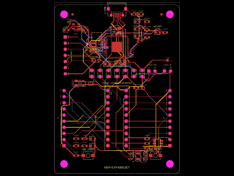 More from this authorShiboSoftwareDev/msp-exp430g2etThis circuit integrates a 4MHz crystal resonator, various resistors and capacitors for power management and filtering, a microcontroller (MSP430F5528), and multiple connectors and test points to enable USB communication, programming, and system monitoring with shielding and grounding.
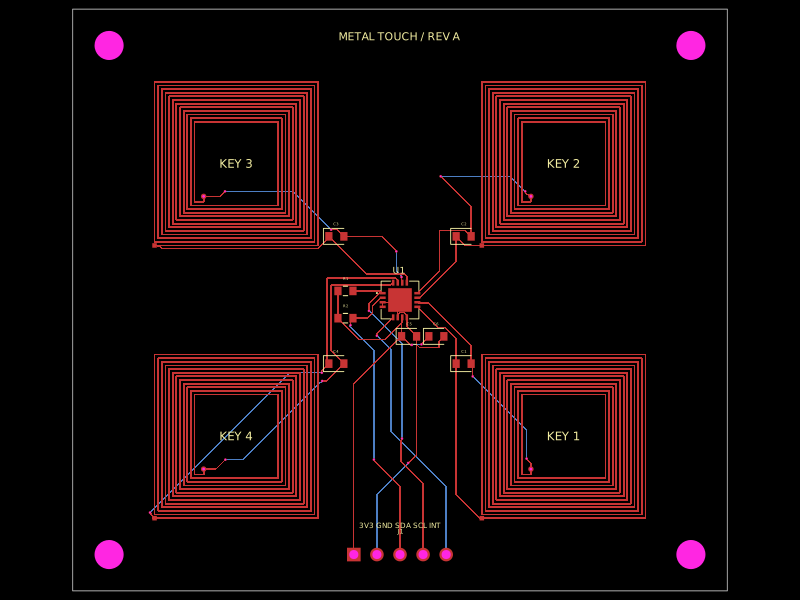 Similar packagehrithik18k/metal-touch-panelA PCB autorouting wrapper that corrects footprint-trace obstacle dimensions, solves routes with a preloaded trace-graph solver, and reports completed traces or routing errors.
 Discover something newpixalynx/usb3-hub-10gA USB 3.2 Gen 2 six-port hub board with USB-C PD power input, regulated 5 V/3.3 V/1.15 V rails, one upstream and four protected downstream USB-A/USB-C ports, SuperSpeed muxes, ESD protection, and controlled port power.