ShiboSoftwareDev/linux-gameboy-advance
Restores PCB assembly metadata by assigning part numbers and 3D CAD models, removing test-point bodies, and validating top-side SMT solder-paste features without altering copper or pads.
- Version
- 1.0.17
- License
- unset
- Stars
- 0
handheld-imports/W25Q16JVUXIQ_Fabrication.tsx
import type { ChipProps } from "@tscircuit/props"

const pinLabels = {
  pin1: ["CS"],
  pin2: ["pin2"],
  pin3: ["pin3"],
  pin4: ["GND"],
  pin5: ["pin5"],
  pin6: ["CLK"],
  pin7: ["pin7"],
  pin8: ["VCC"],
  pin9: ["EP"],
} as const

/** Factory copper/CAD retained; only silkscreen is cleared from exposed lands. */
export const W25Q16JVUXIQ_Fabrication = (props: ChipProps<typeof pinLabels>) => (
  <chip
    pinLabels={pinLabels}
    supplierPartNumbers={{ jlcpcb: ["C2843335"] }}
    manufacturerPartNumber="W25Q16JVUXIQ"
    footprint={
      <footprint>
        <smtpad portHints={["pin1"]} pcbX="-0.750062mm" pcbY="-1.50749mm" width="0.2800096mm" height="0.5999988mm" shape="rect" />
        <smtpad portHints={["pin2"]} pcbX="-0.249936mm" pcbY="-1.50749mm" width="0.2800096mm" height="0.5999988mm" shape="rect" />
        <smtpad portHints={["pin3"]} pcbX="0.249936mm" pcbY="-1.50749mm" width="0.2800096mm" height="0.5999988mm" shape="rect" />
        <smtpad portHints={["pin4"]} pcbX="0.750062mm" pcbY="-1.50749mm" width="0.2800096mm" height="0.5999988mm" shape="rect" />
        <smtpad portHints={["pin8"]} pcbX="-0.750062mm" pcbY="1.50749mm" width="0.2800096mm" height="0.5999988mm" shape="rect" />
        <smtpad portHints={["pin7"]} pcbX="-0.249936mm" pcbY="1.50749mm" width="0.2800096mm" height="0.5999988mm" shape="rect" />
        <smtpad portHints={["pin6"]} pcbX="0.249936mm" pcbY="1.50749mm" width="0.2800096mm" height="0.5999988mm" shape="rect" />
        <smtpad portHints={["pin5"]} pcbX="0.750062mm" pcbY="1.50749mm" width="0.2800096mm" height="0.5999988mm" shape="rect" />
        <smtpad portHints={["pin9"]} pcbX="0mm" pcbY="0mm" width="1.6999966mm" height="0.2999994mm" shape="rect" />
        <silkscreenpath strokeWidth="0.15mm" route={[{ x: 1.15, y: -1.5760446000000456 }, { x: 1.15, y: 1.5763240000001133 }]} />
        <silkscreenpath strokeWidth="0.15mm" route={[{ x: -1.15, y: 1.5763240000001133 }, { x: -1.15, y: -1.5760446000000456 }]} />
        <silkscreencircle pcbX={-0.762} pcbY={-2.19} radius={0.100076} strokeWidth="0.15mm" />
        <silkscreentext text="{NAME}" pcbX="0.003556mm" pcbY="2.813306mm" anchorAlignment="center" fontSize="1mm" />
        <courtyardoutline outline={[{ x: -1.3259439999999358, y: 2.0633060000000114 }, { x: 1.333056000000056, y: 2.0633060000000114 }, { x: 1.333056000000056, y: -2.3736939999998867 }, { x: -1.3259439999999358, y: -2.3736939999998867 }, { x: -1.3259439999999358, y: 2.0633060000000114 }]} />
      </footprint>
    }
    cadModel={{
      objUrl: "https://modelcdn.tscircuit.com/easyeda_models/assets/C2843335.obj?uuid=2b35e1c3dcc44b77887d4f445b51370a",
      stepUrl: "https://modelcdn.tscircuit.com/easyeda_models/assets/C2843335.step?uuid=2b35e1c3dcc44b77887d4f445b51370a",
      pcbRotationOffset: 0,
      modelOriginPosition: { x: 0, y: 0, z: 0 },
    }}
    {...props}
  />
)
Related Packages
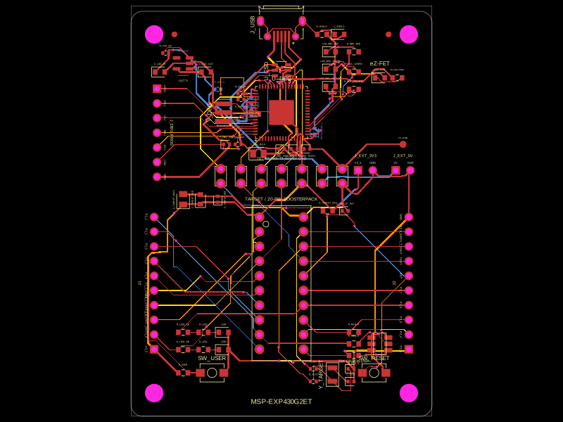 More from this authorShiboSoftwareDev/msp-exp430g2etThis circuit integrates a 4MHz crystal resonator, various resistors and capacitors for power management and filtering, a microcontroller (MSP430F5528), and multiple connectors and test points to enable USB communication, programming, and system monitoring with shielding and grounding.
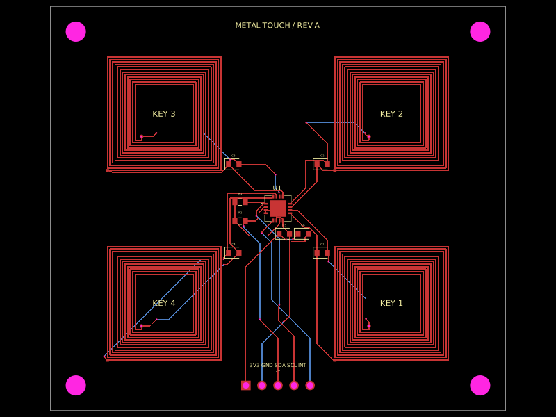 Similar packagehrithik18k/metal-touch-panelA PCB autorouting wrapper that corrects footprint-trace obstacle dimensions, solves routes with a preloaded trace-graph solver, and reports completed traces or routing errors.
 Discover something newpixalynx/usb3-hub-10gA USB 3.2 Gen 2 six-port hub board with USB-C PD power input, regulated 5 V/3.3 V/1.15 V rails, one upstream and four protected downstream USB-A/USB-C ports, SuperSpeed muxes, ESD protection, and controlled port power.