ShiboSoftwareDev/linux-gameboy-advance
Restores PCB assembly metadata by assigning part numbers and 3D CAD models, removing test-point bodies, and validating top-side SMT solder-paste features without altering copper or pads.
- Version
- 1.0.17
- License
- unset
- Stars
- 0
handheld-imports/TPS63070RNMR.tsx
import type { ChipProps } from "@tscircuit/props"

const pinLabels = {
  // TI SLVSC58B, Table 6: pins 7/8 and 12/13 are internally shared.
  // Preserve the exact imported bridged land pattern and expose both aliases.
  pin1: ["PS_SYNC"],
  pin2: ["PG"],
  pin3: ["VAUX", "Vaux"],
  pin4: ["GND"],
  pin5: ["FB"],
  pin6: ["FB2"],
  pin7: ["VOUT", "Vout", "pin8"],
  pin9: ["L2"],
  pin10: ["PGND"],
  pin11: ["L1"],
  pin12: ["VIN", "Vin", "pin13"],
  pin14: ["EN"],
  pin15: ["VSEL", "Vsel"]
} as const

const pinAttributes = {
  pin4: {requiresGround: true},
  pin10: {requiresGround: true},
  pin12: {requiresPower: true}
} as const

export const TPS63070RNMR = (props: ChipProps<typeof pinLabels>) => {
  return (
    <chip
      pinLabels={pinLabels}
      pinAttributes={pinAttributes}
      supplierPartNumbers={{
  "jlcpcb": [
    "C109322"
  ]
}}
      manufacturerPartNumber="TPS63070RNMR"
      footprint={<footprint>
        <smtpad portHints={["pin1"]} pcbX="-0.749935mm" pcbY="-1.1478514mm" width="0.2500122mm" height="0.5999988mm" shape="rect" />
<smtpad portHints={["pin2"]} pcbX="-0.250063mm" pcbY="-1.1475974mm" width="0.2500122mm" height="0.5999988mm" shape="rect" />
<smtpad portHints={["pin3"]} pcbX="0.250063mm" pcbY="-1.1475974mm" width="0.2500122mm" height="0.5999988mm" shape="rect" />
<smtpad portHints={["pin4"]} pcbX="0.749935mm" pcbY="-1.1475974mm" width="0.2500122mm" height="0.5999988mm" shape="rect" />
<smtpad portHints={["pin5"]} pcbX="1.399921mm" pcbY="-0.7225538mm" width="0.5999988mm" height="0.2500122mm" shape="rect" />
<smtpad portHints={["pin6"]} pcbX="1.399921mm" pcbY="-0.2226818mm" width="0.5999988mm" height="0.2500122mm" shape="rect" />
<smtpad portHints={["pin7"]} pcbX="1.399921mm" pcbY="0.2774442mm" width="0.5999988mm" height="0.2500122mm" shape="rect" />
<smtpad portHints={["pin7"]} pcbX="1.400175mm" pcbY="0.7775702mm" width="0.5999988mm" height="0.2500122mm" shape="rect" />
<smtpad portHints={["pin9"]} pcbX="0.499999mm" pcbY="0.7726426mm" width="0.2500122mm" height="1.35001mm" shape="rect" />
<smtpad portHints={["pin10"]} pcbX="0.000127mm" pcbY="0.5478526mm" width="0.2500122mm" height="1.7999964mm" shape="rect" />
<smtpad portHints={["pin11"]} pcbX="-0.499999mm" pcbY="0.7726426mm" width="0.2500122mm" height="1.35001mm" shape="rect" />
<smtpad portHints={["pin12"]} pcbX="-1.400175mm" pcbY="0.7775702mm" width="0.5999988mm" height="0.2500122mm" shape="rect" />
<smtpad portHints={["pin12"]} pcbX="-1.400175mm" pcbY="0.2774442mm" width="0.5999988mm" height="0.2500122mm" shape="rect" />
<smtpad portHints={["pin14"]} pcbX="-1.399921mm" pcbY="-0.2221738mm" width="0.5999988mm" height="0.2500122mm" shape="rect" />
<smtpad portHints={["pin15"]} pcbX="-1.400175mm" pcbY="-0.7222998mm" width="0.5999988mm" height="0.2500122mm" shape="rect" />
<smtpad portHints={["pin12"]} pcbX="-1.225169mm" pcbY="0.5276342mm" width="0.2500122mm" height="0.7500112mm" shape="rect" />
<smtpad portHints={["pin7"]} pcbX="1.225169mm" pcbY="0.5276342mm" width="0.2500122mm" height="0.7500112mm" shape="rect" />
<silkscreenpath route={[{"x":-0.8560816000000386,"y":1.2276581999999507},{"x":-1.4999462000000676,"y":1.2276581999999507}]} />
<silkscreenpath route={[{"x":-1.4999462000000676,"y":-1.2723368000000619},{"x":-1.1061191999999664,"y":-1.2723368000000619}]} />
<silkscreenpath route={[{"x":1.1061445999998796,"y":-1.2723368000000619},{"x":1.5000478000000612,"y":-1.2723368000000619}]} />
<silkscreenpath route={[{"x":1.5000478000000612,"y":-1.2723368000000619},{"x":1.5000478000000612,"y":-1.103553799999986}]} />
<silkscreenpath route={[{"x":1.5000478000000612,"y":1.1087861999999404},{"x":1.5000478000000612,"y":1.2276581999999507}]} />
<silkscreenpath route={[{"x":1.5000478000000612,"y":1.2276581999999507},{"x":0.8561831999999185,"y":1.2276581999999507}]} />
<silkscreenpath route={[{"x":-1.4999462000000676,"y":1.2276581999999507},{"x":-1.4999462000000676,"y":1.1087861999999404}]} />
<silkscreenpath route={[{"x":-1.4999462000000676,"y":-1.103553799999986},{"x":-1.4999462000000676,"y":-1.2723368000000619}]} />
<silkscreencircle pcbX="-0.789813mm" pcbY="-1.7970754mm" radius="0.059944mm" />
<silkscreentext text="{NAME}" pcbX="-0.010795mm" pcbY="2.4454886mm" anchorAlignment="center" fontSize="1mm" />
<courtyardoutline outline={[{"x":-1.9625950000000785,"y":1.695488599999976},{"x":1.9410050000000183,"y":1.695488599999976},{"x":1.9410050000000183,"y":-2.106511399999931},{"x":-1.9625950000000785,"y":-2.106511399999931},{"x":-1.9625950000000785,"y":1.695488599999976}]} />
      </footprint>}
      cadModel={{
        objUrl: "https://modelcdn.tscircuit.com/easyeda_models/assets/C109322.obj?uuid=9c311060aa57458ea4fd5ee4f53427d6",
        stepUrl: "https://modelcdn.tscircuit.com/easyeda_models/assets/C109322.step?uuid=9c311060aa57458ea4fd5ee4f53427d6",
        pcbRotationOffset: 90,
        modelOriginPosition: { x: -0.002247899999929359, y: 0, z: 0 },
      }}
      {...props}
    />
  )
}
Related Packages
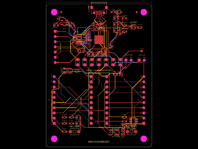 More from this authorShiboSoftwareDev/msp-exp430g2etThis circuit integrates a 4MHz crystal resonator, various resistors and capacitors for power management and filtering, a microcontroller (MSP430F5528), and multiple connectors and test points to enable USB communication, programming, and system monitoring with shielding and grounding.
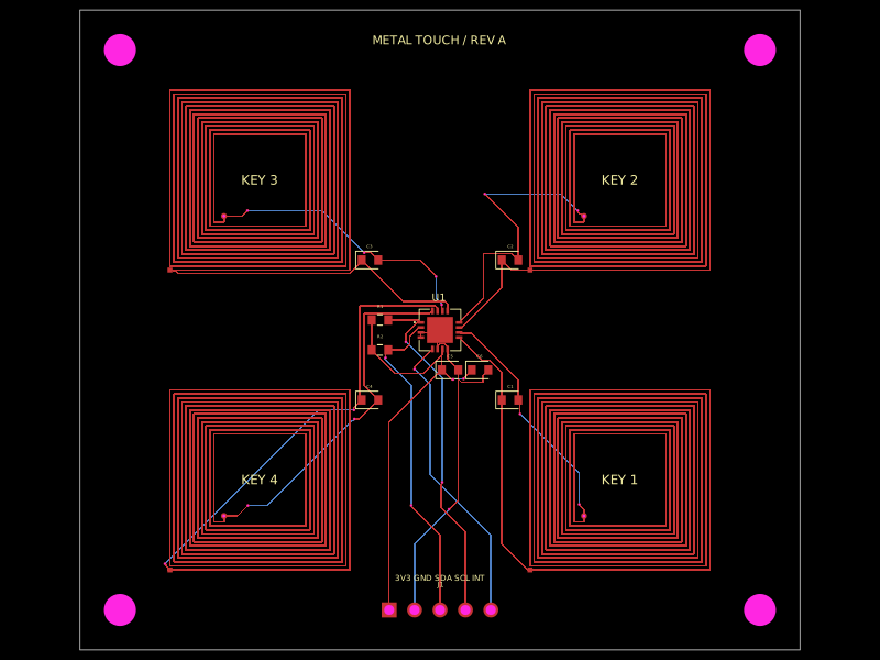 Similar packagehrithik18k/metal-touch-panelA PCB autorouting wrapper that corrects footprint-trace obstacle dimensions, solves routes with a preloaded trace-graph solver, and reports completed traces or routing errors.
 Discover something newpixalynx/usb3-hub-10gA USB 3.2 Gen 2 six-port hub board with USB-C PD power input, regulated 5 V/3.3 V/1.15 V rails, one upstream and four protected downstream USB-A/USB-C ports, SuperSpeed muxes, ESD protection, and controlled port power.