ShiboSoftwareDev/linux-gameboy-advance
Restores PCB assembly metadata by assigning part numbers and 3D CAD models, removing test-point bodies, and validating top-side SMT solder-paste features without altering copper or pads.
- Version
- 1.0.17
- License
- unset
- Stars
- 0
handheld-imports/TF_01A_Fabrication.tsx
import type { ConnectorProps } from "@tscircuit/props"

const pinLabels = {
  pin1: ["DAT2"],
  pin2: ["CD_DAT3"],
  pin3: ["CMD"],
  pin4: ["VDD"],
  pin5: ["CLK"],
  pin6: ["VSS"],
  pin7: ["DAT0"],
  pin8: ["DAT1"],
  pin9: ["CD"],
  pin10: ["SHIELD1"],
  pin11: ["SHIELD4"],
  pin12: ["SHIELD3"],
  pin13: ["SHIELD2"],
} as const

const pinAttributes = {
  pin4: { requiresPower: true },
  pin6: { requiresGround: true },
  pin10: { requiresGround: true },
  pin11: { requiresGround: true },
  pin12: { requiresGround: true },
  pin13: { requiresGround: true },
} as const

// Imported normally from JLC C91145. HRO TF-01A Rev A (2014/9/29)
// recommends nine 0.70 x 1.30 mm signal lands; EasyEDA imports them as 0.60 mm.
// Only their widths are corrected here. Centers, shell lands, NPTHs and CAD
// retain the exact import. The manufacturer drawing specifies no no-pattern area.
// https://datasheet.lcsc.com/datasheet/pdf/7650eac21a54674b08ad4ba21e17fceb.pdf?productCode=C91145
export const TF_01A_Fabrication = (props: ConnectorProps) => (
  <connector
    pinLabels={pinLabels}
    pinAttributes={pinAttributes}
    supplierPartNumbers={{ jlcpcb: ["C91145"] }}
    manufacturerPartNumber="TF-01A"
    footprint={
      <footprint insertionDirection="from_above">
        <hole pcbX="-4.9499393mm" pcbY="-5.39108015mm" diameter="0.999998mm" />
        <hole pcbX="3.0500447mm" pcbY="-5.39108015mm" diameter="0.999998mm" />
        <smtpad portHints={["pin1"]} pcbX="2.2400133mm" pcbY="5.45108765mm" width="0.7mm" height="1.2999974mm" shape="rect" />
        <smtpad portHints={["pin2"]} pcbX="1.1399647mm" pcbY="5.45108765mm" width="0.7mm" height="1.2999974mm" shape="rect" />
        <smtpad portHints={["pin3"]} pcbX="0.0399161mm" pcbY="5.45108765mm" width="0.7mm" height="1.2999974mm" shape="rect" />
        <smtpad portHints={["pin4"]} pcbX="-1.0601325mm" pcbY="5.45108765mm" width="0.7mm" height="1.2999974mm" shape="rect" />
        <smtpad portHints={["pin5"]} pcbX="-2.1599525mm" pcbY="5.45108765mm" width="0.7mm" height="1.2999974mm" shape="rect" />
        <smtpad portHints={["pin6"]} pcbX="-3.2600011mm" pcbY="5.45108765mm" width="0.7mm" height="1.2999974mm" shape="rect" />
        <smtpad portHints={["pin7"]} pcbX="-4.3600497mm" pcbY="5.45108765mm" width="0.7mm" height="1.2999974mm" shape="rect" />
        <smtpad portHints={["pin8"]} pcbX="-5.4598697mm" pcbY="5.45108765mm" width="0.7mm" height="1.2999974mm" shape="rect" />
        <smtpad portHints={["pin9"]} pcbX="-6.5599691mm" pcbY="5.45068125mm" width="0.7mm" height="1.2999974mm" shape="rect" />
        <smtpad portHints={["pin10"]} pcbX="-7.7599667mm" pcbY="4.60069565mm" width="1.1999976mm" height="1.3999972mm" shape="rect" />
        <smtpad portHints={["pin13"]} pcbX="6.9200141mm" pcbY="4.60069565mm" width="1.1999976mm" height="1.3999972mm" shape="rect" />
        <smtpad portHints={["pin12"]} pcbX="7.7599667mm" pcbY="-5.10108835mm" width="1.1999976mm" height="1.999996mm" shape="rect" />
        <smtpad portHints={["pin11"]} pcbX="-7.7599667mm" pcbY="-5.10108835mm" width="1.1999976mm" height="1.999996mm" shape="rect" />
        <silkscreenpath route={[
          { x: -7.365987300000029, y: 3.581139650000182 },
          { x: -7.365987300000029, y: -3.927989349999848 },
        ]} />
        <silkscreenpath route={[
          { x: 7.366012699999828, y: -3.991514749999851 },
          { x: 7.366012699999828, y: 3.501485250000087 },
        ]} />
        <silkscreenpath route={[
          { x: -7.365987300000029, y: -6.340963949999946 },
          { x: -7.365987300000029, y: -9.401054349999981 },
          { x: 7.366012699999828, y: -9.401028949999954 },
          { x: 7.366012699999828, y: -6.491027149999923 },
        ]} />
        <silkscreenpath route={[
          { x: -7.365987300000029, y: -8.915685749999966 },
          { x: -7.365987300000029, y: -8.691022750000116 },
          { x: 1.000010699999848, y: -8.691022750000116 },
          { x: 3.9370126999999684, y: -9.388100349999945 },
        ]} />
        <silkscreentext text="{NAME}" pcbX="0.0000127mm" pcbY="7.11097965mm" anchorAlignment="center" fontSize="1mm" />
        <fabricationnotepath route={[
          { x: -6.999998699999992, y: -9.490995750000025 },
          { x: -6.999998699999992, y: 2.0090066500000603 },
          { x: -6.999998699999992, y: -9.490995750000025 },
        ]} strokeWidth="0.254mm" />
        <fabricationnotepath route={[
          { x: 7.000024100000019, y: -9.490995750000025 },
          { x: 7.000024100000019, y: 2.0090066500000603 },
          { x: 6.0000007000001006, y: 2.0090066500000603 },
          { x: 6.0000007000001006, y: -9.490995750000025 },
          { x: 7.000024100000019, y: -9.490995750000025 },
        ]} strokeWidth="0.254mm" />
        <fabricationnotepath route={[
          { x: -5.999975300000074, y: 2.0090066500000603 },
          { x: 6.0000007000001006, y: 2.0090066500000603 },
          { x: 6.0000007000001006, y: 1.0090086500000552 },
          { x: -5.999975300000074, y: 1.0090086500000552 },
          { x: -5.999975300000074, y: 2.0090066500000603 },
        ]} strokeWidth="0.254mm" />
        <courtyardoutline outline={[
          { x: -8.606587300000115, y: 6.360979650000104 },
          { x: 8.606612699999914, y: 6.360979650000104 },
          { x: 8.606612699999914, y: -9.73462035 },
          { x: -8.606587300000115, y: -9.73462035 },
          { x: -8.606587300000115, y: 6.360979650000104 },
        ]} />
      </footprint>
    }
    cadModel={{
      objUrl: "https://modelcdn.tscircuit.com/easyeda_models/assets/C91145.obj?uuid=5685a23adc9a4e3e9b914abe5ae03aae",
      stepUrl: "https://modelcdn.tscircuit.com/easyeda_models/assets/C91145.step?uuid=5685a23adc9a4e3e9b914abe5ae03aae",
      pcbRotationOffset: 0,
      modelOriginPosition: { x: -0.0022224999997728645, y: 5.101310850000045, z: -0.14733820000000009 },
    }}
    {...props}
  />
)
Related Packages
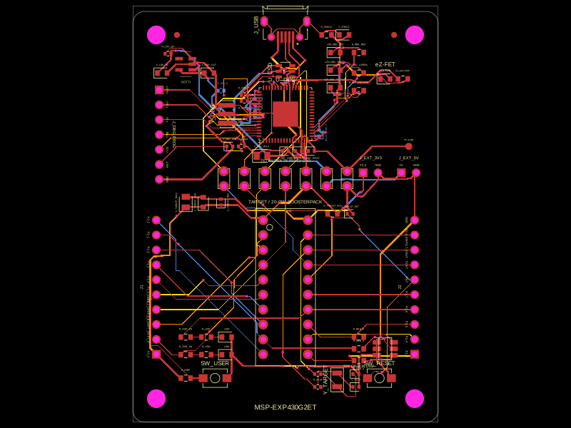 More from this authorShiboSoftwareDev/msp-exp430g2etThis circuit integrates a 4MHz crystal resonator, various resistors and capacitors for power management and filtering, a microcontroller (MSP430F5528), and multiple connectors and test points to enable USB communication, programming, and system monitoring with shielding and grounding.
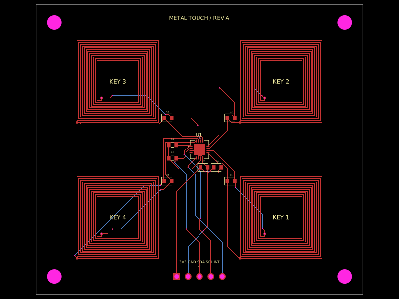 Similar packagehrithik18k/metal-touch-panelA PCB autorouting wrapper that corrects footprint-trace obstacle dimensions, solves routes with a preloaded trace-graph solver, and reports completed traces or routing errors.
 Discover something newpixalynx/usb3-hub-10gA USB 3.2 Gen 2 six-port hub board with USB-C PD power input, regulated 5 V/3.3 V/1.15 V rails, one upstream and four protected downstream USB-A/USB-C ports, SuperSpeed muxes, ESD protection, and controlled port power.