ShiboSoftwareDev/linux-gameboy-advance
Restores PCB assembly metadata by assigning part numbers and 3D CAD models, removing test-point bodies, and validating top-side SMT solder-paste features without altering copper or pads.
- Version
- 1.0.17
- License
- unset
- Stars
- 0
fabrication/README.md
# F1C100S Linux Game Boy Advance fabrication package

Generated from the final verified four-layer 144.5 × 82 mm handheld design. The
package contains top, bottom, and two inner copper Gerbers; solder mask, paste,
silkscreen, fabrication, outline, plated drill, non-plated drill, BOM, and
pick-and-place files. `board-gerbers.zip` contains the complete JLCPCB upload.
The D-pad, A/B/X/Y, Start, and Select controls use the 15 mm actuator
`KH_6X6X15H_SMT_FS_D` (`C18186519`) switch from the verified Game Boy
reference. L/R use `TS66135ZJ 022` (`C33543626`), the 13.5 mm long-stem
variant of the same low-profile 7.3 × 6.1 mm edge-facing switch family as the
original. Their housings finish flush with the PCB edge; only the round stems
protrude 9.6 mm beyond it.
The bottom edge includes a 5 mm-wide, rounded, non-plated battery-cable
cutout beside `J_BAT`; the right-facing connector leaves a 5.95 mm cable-bend
corridor before the slot. The cutout extends 9.5 mm into the PCB and is emitted directly
in `Edge_Cuts.gbr` rather than as an unsupported non-round drill. The microSD
socket is 0.399 mm behind its dedicated right-edge access bay. The power switch
is recessed 7.4 mm at the lower-left for a guarded enclosure slider, matching the
AGB-001 bottom control arrangement rather than exposing it in the hand grip.

All 120 fitted PCB placements have explicit LCSC/JLCPCB numbers and renderable,
non-placeholder 3D models. The quantity-aware live audit in
`../jlc-availability.json` found sufficient indexed stock for all 51 unique part
numbers on 2026-10-02; inventory is not reserved, so recheck at order time. The
LCD, speaker, and 4×AAA holder are cable-connected mechanical items and are not
PCB placements. The intended ER-TFT035IPS-6 panel has a manufacturer-dimensioned
landscape GLB assembly model, including its active area, panel stack, 50-way
flex, contacts, stiffener, and installed cable rise into right-side `J_LCD`.

Bottom-side JST-SH connectors at the top/rear service edge expose UART
(RX/GND/TX), I²C (GND/3V3/SDA/SCL), and SPI
(GND/3V3/SCLK/MOSI/MISO/CS). `J_SPK` is the differential PAM8403 bridge output
for an internal 4–8 Ω speaker; neither speaker terminal is ground.

Every routed via is 0.30 mm finished hole / 0.45 mm copper pad. The closest
finished-hole edge spacing is 0.202524 mm. The reviewed V3V3 via now has
0.540 mm finished-hole-to-other-net-copper clearance. Both AP63203 output-capacitor
links are physically 0.50 mm wide. The LCD backlight uses an AP3031 regulated
boost driver set to 100 mA. The final circuit has 435 PCB traces, 522 vias, zero
emitted `*_error` records, and passes the independent all-layer Gerber shorts
check. The battery input is specified and labeled 4.8–6.4 V rather than 3.8–6.4 V.

Use a four-layer 1.6 mm FR-4 stack. Review polarity and rotation in JLCPCB's
assembly preview before ordering because the exporter cannot verify supplier
pin-1 orientation. This design has passed software fabrication checks but has
not yet been physically assembled or boot-tested; follow the first-article
bring-up steps in `../README.md`.
Related Packages
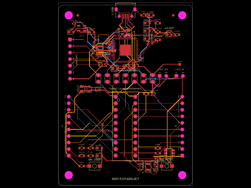 More from this authorShiboSoftwareDev/msp-exp430g2etThis circuit integrates a 4MHz crystal resonator, various resistors and capacitors for power management and filtering, a microcontroller (MSP430F5528), and multiple connectors and test points to enable USB communication, programming, and system monitoring with shielding and grounding.
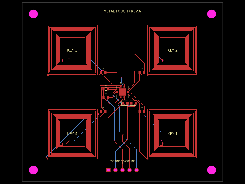 Similar packagehrithik18k/metal-touch-panelA PCB autorouting wrapper that corrects footprint-trace obstacle dimensions, solves routes with a preloaded trace-graph solver, and reports completed traces or routing errors.
 Discover something newpixalynx/usb3-hub-10gA USB 3.2 Gen 2 six-port hub board with USB-C PD power input, regulated 5 V/3.3 V/1.15 V rails, one upstream and four protected downstream USB-A/USB-C ports, SuperSpeed muxes, ESD protection, and controlled port power.