ShiboSoftwareDev/linux-gameboy-advance
Restores PCB assembly metadata by assigning part numbers and 3D CAD models, removing test-point bodies, and validating top-side SMT solder-paste features without altering copper or pads.
- Version
- 1.0.17
- License
- unset
- Stars
- 0
carrier-router.ts
import verifiedCarrierRoutes from "./carrier-routes-v2.json"
import backlightRoutes from "./backlight-routes.json"

type EventName = "complete" | "error" | "progress"
type Handler = (event: any) => void

const wire = (x: number, y: number, width: number, layer: string, extra = {}) => ({
  route_type: "wire",
  x,
  y,
  width,
  layer,
  ...extra,
})

const via = (x: number, y: number, fromLayer: string, toLayer: string) => ({
  route_type: "via",
  x,
  y,
  from_layer: fromLayer,
  to_layer: toLayer,
  via_diameter: 0.45,
  via_hole_diameter: 0.3,
})

/** Apply the small, reviewed clearance corrections to the freshly solved
 * carrier. Keeping them declarative makes the website build deterministic and
 * leaves the 247-route solution easy to reproduce from carrier-routes-v2.json. */
function applyClearanceRepairs(traces: any[]) {
  const byId = new Map(traces.map((trace) => [trace.pcb_trace_id, trace]))
  const endingWith = (suffix: string) => {
    const matches = traces.filter((trace) => trace.pcb_trace_id.endsWith(suffix))
    if (matches.length !== 1)
      throw new Error(`Expected one saved carrier route ending in ${suffix}, found ${matches.length}`)
    return matches[0]
  }

  // The low-profile TS66135ZJ shoulder switches retain the original housing
  // geometry but use 13.5 mm stems. Their bodies finish at the board edge and
  // the actuator tips reach 9.6 mm past it.
  const rightShoulderGround = byId.get("source_net_0_mst45_0")
  rightShoulderGround.connectsTo = ["pcb_port_290", "pcb_port_406"]
  Object.assign(rightShoulderGround.route[1], { x: 39.7, y: 38.149993 })
  Object.assign(rightShoulderGround.route.at(-1), { x: 42.749941, y: 38.149993 })
  rightShoulderGround.route.at(-1).end_pcb_port_id = "pcb_port_406"

  const leftShoulderGround = byId.get("source_net_0_mst85_0")
  leftShoulderGround.connectsTo = ["pcb_port_402", "pcb_port_493"]
  Object.assign(leftShoulderGround.route[0], { x: -47.250059, y: 38.149993 })
  leftShoulderGround.route[0].start_pcb_port_id = "pcb_port_402"
  Object.assign(leftShoulderGround.route[1], { x: -46.75, y: 38.149993 })

  const leftShoulderSignal = byId.get("source_trace_242_0")
  leftShoulderSignal.connectsTo = ["pcb_port_403", "pcb_port_350"]
  Object.assign(leftShoulderSignal.route[0], { x: -42.749941, y: 38.149993 })
  leftShoulderSignal.route[0].start_pcb_port_id = "pcb_port_403"
  const rightShoulderSignal = byId.get("source_trace_244_0")
  rightShoulderSignal.connectsTo = ["pcb_port_407", "pcb_port_351"]
  Object.assign(rightShoulderSignal.route[0], { x: 47.250059, y: 38.149993 })
  rightShoulderSignal.route[0].start_pcb_port_id = "pcb_port_407"

  // Move J_BAT left while preserving its right-facing orientation. The JST-PH
  // housing now stops 5.95 mm before the cable cutout, leaving a real wire-bend
  // corridor instead of placing the plug directly against the routed slot.
  byId.get("source_net_2_0").route = [
    wire(-40, -38.37499805, 0.5, "top", { start_pcb_port_id: "pcb_port_438" }),
    wire(-41.2, -38.37499805, 0.5, "top"),
    wire(-41.2, -33, 0.5, "top"),
    wire(-39.853438, -31, 0.5, "top", { end_pcb_port_id: "pcb_port_440" }),
  ]

  byId.get("source_net_0_mst68_0").route = [
    wire(-40, -36.37500205, 0.5, "top", { start_pcb_port_id: "pcb_port_439" }),
    wire(-39.5, -35.87500205, 0.5, "top"),
    wire(-31.5625, -34.53750128125, 0.5, "top"),
    wire(-31.5625, -28.5625, 0.5, "top"),
    wire(-30, -27, 0.5, "top", { end_pcb_port_id: "pcb_port_466" }),
  ]

  // Relocate the power control to the lower edge, matching the original GBA's
  // protected bottom control strip. Its actuator is recessed behind the board
  // edge, while the high-current battery path remains 0.5 mm throughout.
  byId.get("source_net_3_0").route = [
    wire(-36.146562, -31, 0.5, "top", { start_pcb_port_id: "pcb_port_441" }),
    wire(-34.5, -28.5, 0.5, "top"),
    via(-34.5, -28.5, "top", "inner1"),
    wire(-34.5, -28.5, 0.5, "inner1"),
    wire(-50, -28, 0.5, "inner1"),
    wire(-58.325, -32.5, 0.5, "inner1", { end_pcb_port_id: "pcb_port_442" }),
  ]
  byId.get("source_net_4_0").route = [
    wire(-61.373, -32.5, 0.5, "inner2", { start_pcb_port_id: "pcb_port_443" }),
    wire(-61.373, -40.2, 0.5, "inner2"),
    wire(-35, -40.2, 0.5, "inner2"),
    wire(-35, -34.5, 0.5, "inner2"),
    via(-35, -34.5, "inner2", "top"),
    wire(-35, -34.5, 0.5, "top"),
    wire(-33.199894, -31, 0.5, "top", { end_pcb_port_id: "pcb_port_448" }),
  ]
  byId.get("source_net_0_mst78_0").route = [
    wire(-56.200017, -21.249805, 0.5, "top", { start_pcb_port_id: "pcb_port_395" }),
    wire(-68.75, -24.5, 0.5, "top"),
    wire(-68.75, -31.75, 0.5, "top"),
    wire(-67.977, -32.5, 0.5, "top", { end_pcb_port_id: "pcb_port_445" }),
  ]
  byId.get("source_net_0_mst82_0").route = [
    wire(-67.977, -32.5, 0.5, "top", { start_pcb_port_id: "pcb_port_445" }),
    wire(-67, -34.5, 0.5, "top"),
    wire(-56, -34.5, 0.5, "top"),
    wire(-55.023, -32.5, 0.5, "top", { end_pcb_port_id: "pcb_port_446" }),
  ]

  // Keep this short ground link at the board minimum width. The autorouter's
  // global ground expansion otherwise encroaches on adjacent VCI pin 42.
  byId.get("source_net_0_mst8_0").route = byId
    .get("source_net_0_mst8_0")
    .route.map((point: any) => ({ ...point, width: 0.12 }))

  // The SimpleRouteJson converter omits the connector's two non-plated shell
  // holes. Take the shield-to-shield ground link below both 0.6 mm drills.
  byId.get("source_net_0_mst39_0").route = [
    wire(-3.1999555, -34.3259568, 0.5, "top", { start_pcb_port_id: "pcb_port_422" }),
    wire(-4, -35.1259568, 0.5, "top"),
    wire(-4, -36.6, 0.5, "top"),
    wire(4, -36.6, 0.5, "top"),
    wire(4, -35.1258552, 0.5, "top"),
    wire(3.2000063, -34.3258552, 0.5, "top", { end_pcb_port_id: "pcb_port_423" }),
  ]

  // A long LCD signal passes a fixed VCC_DRAM module via. Move only its
  // inner-layer elbow; all terminal and layer transitions remain.
  const lcdPe5 = byId.get("source_trace_125_0")
  lcdPe5.route.splice(
    2,
    1,
    wire(-9.9, -10.8, 0.12, "inner1"),
    wire(-7.564621678403883, -12.742778726988721, 0.12, "inner1"),
  )

  // JLCPCB measures via-hole-to-copper spacing from the finished drill edge.
  // This V3V3 via used to leave only 0.177 mm to the module's inner2 HPL
  // trace. Drop the transition below that elbow while retaining both layers
  // and the original endpoints; the resulting finished-hole clearance is over
  // the published 0.20 mm minimum.
  const v3v3ClearanceRoute = endingWith("source_net_6_mst40_0")
  for (const point of v3v3ClearanceRoute.route.slice(2, 5)) {
    point.x = 8.399
    point.y = 10.65
  }

  // The solved carrier reduced the regulator's 0.5 mm output-capacitor links
  // to the 0.12 mm signal minimum. Restore both local switching-current paths
  // to their requested width. The feedback branch remains a short 0.12 mm
  // Kelvin-sense connection, as intended.
  for (const suffix of ["source_net_6_mst14_0", "source_net_6_mst23_0"])
    endingWith(suffix).route = endingWith(suffix).route.map((point: any) =>
      point.route_type === "wire" ? { ...point, width: 0.5 } : point)

  return traces
}

/** Route the rear service connectors explicitly. The saved carrier solution
 * predates these headers, so keeping this small route set beside it makes the
 * published build deterministic while still letting tscircuit run its normal
 * connectivity, clearance, and short checks on every build. */
function createServiceConnectorRoutes() {
  const trace = (
    id: string,
    connectsTo: string[],
    route: any[],
  ) => ({
    type: "pcb_trace",
    pcb_trace_id: id,
    connection_name: id.replace(/_0$/, ""),
    connectsTo,
    route,
  })

  return [
    // UART follows the standard programmer order RX-GND-TX. Rather than
    // crossing the processor escape, both signals join the already-routed
    // UART test-point copper around the quiet left perimeter.
    trace("source_trace_377_0", ["pcb_port_564", "pcb_port_499"], [
      wire(-16.999875, 35.6749963, 0.12, "bottom", { start_pcb_port_id: "pcb_port_564" }),
      wire(-16.7, 35.3, 0.12, "bottom"),
      wire(-16.7, 33.2, 0.12, "bottom"),
      via(-16.7, 33.2, "bottom", "inner1"),
      wire(-16.7, 33.2, 0.12, "inner1"),
      wire(-63.5, 33.2, 0.12, "inner1"),
      wire(-67, 29.7, 0.12, "inner1"),
      wire(-67, -26.2, 0.12, "inner1"),
      wire(-36.5, -26.2, 0.12, "inner1"),
      wire(-39.46, -20, 0.12, "inner1", { end_pcb_port_id: "pcb_port_499" }),
    ]),
    trace("source_trace_379_0", ["pcb_port_566", "pcb_port_498"], [
      wire(-18.999871, 35.6749963, 0.12, "bottom", { start_pcb_port_id: "pcb_port_566" }),
      wire(-19.3, 35.3, 0.12, "bottom"),
      wire(-19.3, 30.8, 0.12, "bottom"),
      via(-19.3, 30.8, "bottom", "inner1"),
      wire(-19.3, 30.8, 0.12, "inner1"),
      wire(-56, 30.8, 0.12, "inner1"),
      wire(-56, 28.8, 0.12, "inner1"),
      wire(-63.2, 28.8, 0.12, "inner1"),
      wire(-66.2, 25.8, 0.12, "inner1"),
      wire(-66.2, -25.5, 0.12, "inner1"),
      wire(-42, -25.5, 0.12, "inner1"),
      wire(-42, -20, 0.12, "inner1", { end_pcb_port_id: "pcb_port_498" }),
    ]),
    // Both expansion headers share one 3V3 branch. The SPI-side leg then joins
    // the existing LCD/SD 3V3 copper, avoiding a second long supply route.
    trace("source_trace_381_0", ["pcb_port_568", "pcb_port_574"], [
      wire(-28.499872, 34.9994833, 0.5, "bottom", { start_pcb_port_id: "pcb_port_568" }),
      wire(-28.5, 33.8, 0.5, "bottom"),
      via(-28.5, 33.8, "bottom", "inner2"),
      wire(-28.5, 33.8, 0.5, "inner2"),
      wire(-28.5, 35.5, 0.5, "inner2"),
      wire(20.5, 35.5, 0.5, "inner2"),
      wire(20.5, 33.8, 0.5, "inner2"),
    ]),
    // Route I2C across the open top strip, then approach the two LCD control
    // pads from the connector's clear right-hand side.
    trace("source_trace_382_0", ["pcb_port_569", "pcb_port_284"], [
      wire(-27.49962, 34.9999913, 0.12, "bottom", { start_pcb_port_id: "pcb_port_569" }),
      wire(-27.5, 32.5, 0.12, "bottom"),
      via(-27.5, 32.5, "bottom", "inner2"),
      wire(-27.5, 32.5, 0.12, "inner2"),
      // Briefly use the top layer to pass below the clustered SPI and 3V3
      // vias. Keeping the long sections at y=32.5 also clears the UART via.
      wire(17, 32.5, 0.12, "inner2"),
      via(17, 32.5, "inner2", "top"),
      wire(17, 32.5, 0.12, "top"),
      wire(17, 31.5, 0.12, "top"),
      wire(22.7, 31.5, 0.12, "top"),
      wire(22.7, 32.5, 0.12, "top"),
      via(22.7, 32.5, "top", "inner2"),
      wire(22.7, 32.5, 0.12, "inner2"),
      wire(47.4, 32.5, 0.12, "inner2"),
      wire(47.4, 24.606427015, 0.12, "inner2"),
      wire(40.657547168, 24.606427015, 0.12, "inner2"),
    ]),
    trace("source_trace_383_0", ["pcb_port_570", "pcb_port_283"], [
      wire(-26.499622, 34.9999913, 0.12, "bottom", { start_pcb_port_id: "pcb_port_570" }),
      wire(-26.5, 31.7, 0.12, "bottom"),
      via(-26.5, 31.7, "bottom", "inner2"),
      wire(-26.5, 31.7, 0.12, "inner2"),
      wire(46, 31.7, 0.12, "inner2"),
      wire(46, 25.3, 0.12, "inner2"),
      via(46, 25.3, "inner2", "inner1"),
      wire(46, 25.3, 0.12, "inner1"),
      wire(46, 24, 0.12, "inner1"),
      via(46, 24, "inner1", "inner2"),
      wire(46, 24, 0.12, "inner2"),
      wire(46, 23.430917565, 0.12, "inner2"),
      wire(43.439988568, 23.430917565, 0.12, "inner2"),
    ]),
    // Join 3V3 at the existing through-via feeding the LCD/SD supply branch.
    trace("source_trace_387_0", ["pcb_port_574", "pcb_port_292"], [
      wire(20.500257, 34.9499914, 0.5, "bottom", { start_pcb_port_id: "pcb_port_574" }),
      wire(20.5, 33.8, 0.5, "bottom"),
      via(20.5, 33.8, "bottom", "top"),
      wire(20.5, 33.8, 0.5, "top"),
      wire(33.675, 33.8, 0.5, "top"),
      wire(33.675, 22, 0.5, "top", { end_pcb_port_id: "pcb_port_292" }),
    ]),
    // The four SPI stubs land directly on open sections of the existing LCD
    // serial-control routes. This is electrically identical to routing to the
    // FPC pads, but avoids disturbing the dense 0.5 mm-pitch fanout.
    trace("source_trace_388_0", ["pcb_port_575", "pcb_port_275"], [
      wire(21.500255, 34.9499914, 0.12, "bottom", { start_pcb_port_id: "pcb_port_575" }),
      wire(21.500255, 31.007408282, 0.12, "bottom"),
      via(21.500255, 31.007408282, "bottom", "top"),
      wire(21.500255, 31.007408282, 0.12, "top"),
    ]),
    trace("source_trace_389_0", ["pcb_port_576", "pcb_port_273"], [
      wire(22.500253, 34.9499914, 0.12, "bottom", { start_pcb_port_id: "pcb_port_576" }),
      wire(22.500253, 36, 0.12, "bottom"),
      wire(18, 36, 0.12, "bottom"),
      wire(18, 32.3, 0.12, "bottom"),
      via(18, 32.3, "bottom", "inner1"),
      wire(18, 32.3, 0.12, "inner1"),
      wire(18, 28.442000206, 0.12, "inner1"),
      via(18, 28.442000206, "inner1", "inner2"),
      wire(18, 28.442000206, 0.12, "inner2"),
    ]),
    trace("source_trace_390_0", ["pcb_port_577", "pcb_port_272"], [
      wire(23.500251, 34.9499914, 0.12, "bottom", { start_pcb_port_id: "pcb_port_577" }),
      wire(23.500251, 33, 0.12, "bottom"),
      via(23.500251, 33, "bottom", "inner1"),
      wire(23.500251, 33, 0.12, "inner1"),
      wire(19, 33, 0.12, "inner1"),
      wire(19, 25.703043614, 0.12, "inner1"),
    ]),
    trace("source_trace_391_0", ["pcb_port_578", "pcb_port_277"], [
      wire(24.500249, 34.9499914, 0.12, "bottom", { start_pcb_port_id: "pcb_port_578" }),
      wire(24.500249, 36.682, 0.12, "bottom"),
      wire(20.44983163, 36.682, 0.12, "bottom"),
      via(20.44983163, 36.682, "bottom", "inner1"),
      wire(20.44983163, 36.682, 0.12, "inner1"),
    ]),
  ]
}

/** Replays the checked carrier solution. Every build still runs tscircuit's
 * copper, connectivity, clearance, DRC, and short-circuit validation. */
class CarrierAutorouter {
  input: any
  isRouting = false
  private handlers: Record<EventName, Handler[]> = {
    complete: [],
    error: [],
    progress: [],
  }

  constructor(input: any) { this.input = input }

  on(event: EventName, callback: Handler) {
    this.handlers[event].push(callback)
  }

  private getTraces() {
    const traces = applyClearanceRepairs(structuredClone(verifiedCarrierRoutes as any[]))
    return [
      ...traces,
      ...structuredClone(backlightRoutes as any[]),
      ...createServiceConnectorRoutes(),
    ]
  }

  start() {
    if (this.isRouting) return
    this.isRouting = true
    queueMicrotask(() => {
      this.isRouting = false
      const event = { type: "complete", traces: this.getTraces() }
      for (const callback of this.handlers.complete) callback(event)
    })
  }

  stop() {
    this.isRouting = false
  }

  solveSync() {
    return this.getTraces()
  }
}

export async function createCarrierAutorouter(simpleRouteJson: any) {
  return new CarrierAutorouter(simpleRouteJson)
}
Related Packages
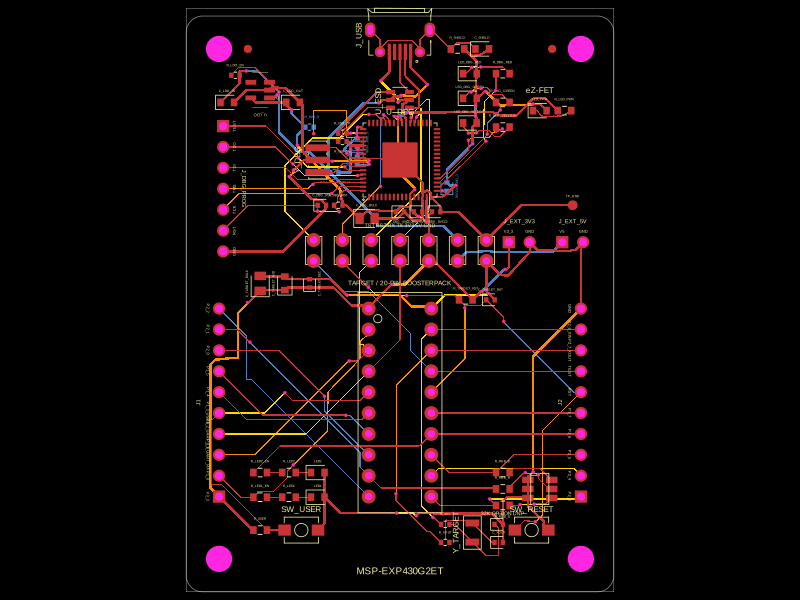 More from this authorShiboSoftwareDev/msp-exp430g2etThis circuit integrates a 4MHz crystal resonator, various resistors and capacitors for power management and filtering, a microcontroller (MSP430F5528), and multiple connectors and test points to enable USB communication, programming, and system monitoring with shielding and grounding.
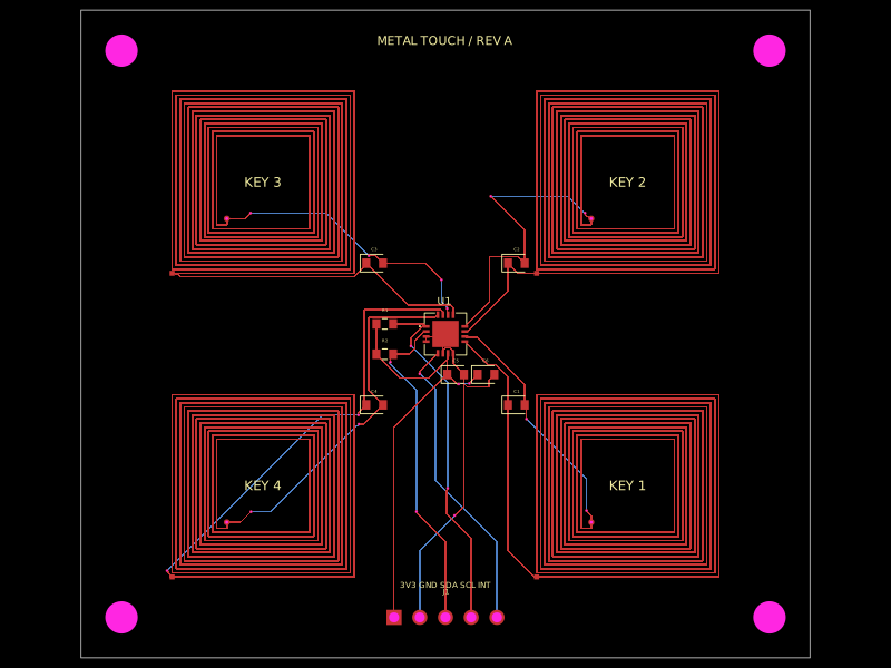 Similar packagehrithik18k/metal-touch-panelA PCB autorouting wrapper that corrects footprint-trace obstacle dimensions, solves routes with a preloaded trace-graph solver, and reports completed traces or routing errors.
 Discover something newpixalynx/usb3-hub-10gA USB 3.2 Gen 2 six-port hub board with USB-C PD power input, regulated 5 V/3.3 V/1.15 V rails, one upstream and four protected downstream USB-A/USB-C ports, SuperSpeed muxes, ESD protection, and controlled port power.