ShiboSoftwareDev/f1c100s-linux-stepper-controller
A four-layer Linux motor-control carrier built around an Allwinner F1C100S SoC, USB‑C, SPI flash, multi-rail power regulation, DRV8825 stepper-driver stage with protection/current sensing, temperature monitoring, and external I/O connectors.
- Version
- 0.1.1
- License
- unset
- Stars
- 0
motor-stage.tsx
import { B4B_PH_K_S_LF__SN_ } from "./imports/B4B_PH_K_S_LF__SN_"
import { DRV8825PWPR } from "./imports/DRV8825PWPR"
import { HoLRT1206_1W_300mR_1_ } from "./imports/HoLRT1206_1W_300mR_1_"
import { PMEG6020ELRX } from "./imports/PMEG6020ELRX"
import { TCJD226M050R0090E } from "./imports/TCJD226M050R0090E"
import { TMP102AIDRLR } from "./imports/TMP102AIDRLR"
import { WJ500V_5_08_2P } from "./imports/WJ500V_5_08_2P"

const signal = { thickness: 0.15 } as const
const ground = { thickness: 0.3 } as const
const power = { thickness: 0.8 } as const
// The phase routes neck to 0.12 mm at the 0.65 mm-pitch driver pins, then the
// frozen board route widens their long trunks to 0.30 mm. Motor input uses 0.8 mm.
const motor = { thickness: 0.12 } as const

const connect = (name: string, from: string, to: string, thickness = 0.15) =>
  <trace name={name} from={from} to={to} thickness={thickness} />

/**
 * A 9–20 V, 0.5 A-peak NEMA-17 stage for the F1C100S Linux carrier.
 * The enable line drives both nRESET and nSLEEP and is pulled down so the
 * bridge cannot energize before Linux explicitly arms it.
 */
export function MotorStage() {
  return <group name="MOTOR_STAGE" pcbX={5} pcbY={0} schX={0} schY={0}>
    <net name="VMOTOR" nominalTraceWidth={0.8} />
    <net name="DRV_VREF" nominalTraceWidth={0.15} />

    <WJ500V_5_08_2P name="J_VM" pcbX={34} pcbY={19} pcbRotation={0}
      schX={52} schY={12} />
    <fuse name="F_VM" currentRating="2A" voltageRating="30V" footprint="1812"
      supplierPartNumbers={{jlcpcb:["C960026"]}} manufacturerPartNumber="BSMD1812-200-30V"
      pcbX={27.3} pcbY={11.3} schX={46} schY={12} />
    <PMEG6020ELRX name="D_VM_BLOCK" pcbX={33} pcbY={11.2} schX={49} schY={12} />
    <chip name="D_VM_TVS" footprint="smb" pcbX={45} pcbY={12.2} pcbRotation={180}
      pinLabels={{pin1:"TVS1",pin2:"TVS2"}}
      supplierPartNumbers={{jlcpcb:["C1975329"]}} manufacturerPartNumber="SMBJ22CAQ-13-F"
      schX={49} schY={8} schRotation={90} />
    <TCJD226M050R0090E name="C_VM_BULK" pcbX={43} pcbY={4.5} pcbRotation={90}
      schX={52} schY={8} schOrientation="vertical" />
    <capacitor name="C_VM_CER" capacitance="10uF" maxVoltageRating="50V" footprint="1206"
      supplierPartNumbers={{jlcpcb:["C13585"]}} manufacturerPartNumber="CL31A106KBHNNNE"
      pcbX={34} pcbY={8.5} schX={55} schY={8} schOrientation="vertical"
      maxDecouplingTraceLength={30} />

    <DRV8825PWPR name="U_MOTOR" noConnect={["DECAY","nHOME","NC"]}
      pcbX={34} pcbY={0} pcbRotation={0} schX={43} schY={0}
      schPinArrangement={{
        leftSide:{pins:[22,20,16,17,18,21,24,25,26],direction:"top-to-bottom"},
        rightSide:{pins:[5,7,10,8,6,9,19,27,23],direction:"top-to-bottom"},
        topSide:{pins:[4,11,1,2,3,15],direction:"left-to-right"},
        bottomSide:{pins:[12,13,14,28,29],direction:"left-to-right"},
      }} />

    {/* Charge pump, motor-rail bypassing, current regulation and safe defaults. */}
    <capacitor name="C_CP" capacitance="10nF" maxVoltageRating="50V" footprint="0402"
      supplierPartNumbers={{jlcpcb:["C15195"]}} pcbX={29.3} pcbY={-4.7} schX={39} schY={6} maxDecouplingTraceLength={25} />
    <capacitor name="C_VCP" capacitance="100nF" maxVoltageRating="50V" footprint="0402"
      supplierPartNumbers={{jlcpcb:["C960916"]}} pcbX={27} pcbY={-2.8} schX={42} schY={6} maxDecouplingTraceLength={25} />
    <resistor name="R_VCP" resistance="1M" footprint="0402"
      supplierPartNumbers={{jlcpcb:["C26083"]}} pcbX={33.4} pcbY={-5.2} schX={45} schY={6} />
    <capacitor name="C_VMA" capacitance="100nF" maxVoltageRating="50V" footprint="0402"
      supplierPartNumbers={{jlcpcb:["C960916"]}} pcbX={31.5} pcbY={-4.8} schX={48} schY={6} maxDecouplingTraceLength={25} />
    <capacitor name="C_VMB" capacitance="100nF" maxVoltageRating="50V" footprint="0402"
      supplierPartNumbers={{jlcpcb:["C960916"]}} pcbX={36.5} pcbY={-4.8} schX={51} schY={6} maxDecouplingTraceLength={25} />
    <capacitor name="C_DRV_3V3" capacitance="470nF" maxVoltageRating="16V" footprint="0402"
      supplierPartNumbers={{jlcpcb:["C480644"]}} pcbX={40.5} pcbY={-4} schX={39} schY={-7} maxDecouplingTraceLength={12} />
    <resistor name="R_REF_TOP" resistance="6.8k" footprint="0402"
      supplierPartNumbers={{jlcpcb:["C25952"]}} pcbX={36} pcbY={5} schX={42} schY={-7} />
    <resistor name="R_REF_BOTTOM" resistance="2k" footprint="0402"
      supplierPartNumbers={{jlcpcb:["C4109"]}} pcbX={34} pcbY={5} schX={45} schY={-7} />
    <capacitor name="C_REF" capacitance="100nF" maxVoltageRating="16V" footprint="0402"
      supplierPartNumbers={{jlcpcb:["C1525"]}} pcbX={32} pcbY={5} schX={48} schY={-7} maxDecouplingTraceLength={25} />
    <resistor name="R_ENABLE_PD" resistance="100k" footprint="0402"
      supplierPartNumbers={{jlcpcb:["C25741"]}} pcbX={27.5} pcbY={0} schX={37} schY={-3} />
    <resistor name="R_FAULT_PU" resistance="10k" footprint="0402"
      supplierPartNumbers={{jlcpcb:["C25744"]}} pcbX={27.5} pcbY={2} schX={37} schY={-5} />
    <HoLRT1206_1W_300mR_1_ name="R_ISEN_A" pcbX={30.5} pcbY={-7.5}
      schX={51} schY={-4} schOrientation="vertical" />
    <HoLRT1206_1W_300mR_1_ name="R_ISEN_B" pcbX={37.5} pcbY={-7.5}
      schX={54} schY={-4} schOrientation="vertical" />

    <B4B_PH_K_S_LF__SN_ name="J_MOTOR" pcbX={34} pcbY={-20.5} pcbRotation={0}
      schX={55} schY={0} />

    {/* TMP102 measures the driver-area board temperature; ALERT is read by PE6. */}
    <TMP102AIDRLR name="U_TEMP" pcbX={30} pcbY={-10.2} pcbRotation={0}
      schX={43} schY={-13} />
    <capacitor name="C_TEMP" capacitance="100nF" maxVoltageRating="16V" footprint="0402"
      supplierPartNumbers={{jlcpcb:["C1525"]}} pcbX={27.5} pcbY={-10.2}
      schX={47} schY={-13} schOrientation="vertical" maxDecouplingTraceLength={25} />
    <resistor name="R_TEMP_ALERT" resistance="10k" footprint="0402"
      supplierPartNumbers={{jlcpcb:["C25744"]}} pcbX={30} pcbY={-12.2}
      schX={39} schY={-13} schOrientation="vertical" />

    {/* Motor input protection and local energy storage. */}
    {connect("VM_INPUT", ".J_VM > .pin1", ".F_VM > .pin1", 0.8)}
    {connect("VM_FUSED", ".F_VM > .pin2", ".D_VM_BLOCK > .anode", power.thickness)}
    {connect("VM_PROTECTED", ".D_VM_BLOCK > .cathode", "net.VMOTOR", power.thickness)}
    {connect("VM_INPUT_GND", ".J_VM > .pin2", "net.BOARD_GND", 0.8)}
    {connect("VM_TVS", ".D_VM_TVS > .pin1", "net.VMOTOR", 0.8)}
    {connect("VM_TVS_GND", ".D_VM_TVS > .pin2", "net.BOARD_GND", 0.8)}
    {connect("VM_BULK", ".C_VM_BULK > .pin1", "net.VMOTOR", 0.8)}
    {connect("VM_BULK_GND", ".C_VM_BULK > .pin2", "net.BOARD_GND", 0.8)}
    {connect("VM_CER", ".C_VM_CER > .pin1", "net.VMOTOR", 0.8)}
    {connect("VM_CER_GND", ".C_VM_CER > .pin2", "net.BOARD_GND", 0.8)}

    {/* DRV8825 supply and charge pump. */}
    {connect("DRV_VMA", ".U_MOTOR > .VMA", "net.VMOTOR", 0.8)}
    {connect("DRV_VMB", ".U_MOTOR > .VMB", "net.VMOTOR", 0.8)}
    {connect("DRV_C_VMA", ".C_VMA > .pin1", ".U_MOTOR > .VMA", 0.12)}
    {connect("DRV_C_VMA_GND", ".C_VMA > .pin2", "net.BOARD_GND", 0.3)}
    {connect("DRV_C_VMB", ".C_VMB > .pin1", ".U_MOTOR > .VMB", 0.12)}
    {connect("DRV_C_VMB_GND", ".C_VMB > .pin2", "net.BOARD_GND", 0.3)}
    {connect("DRV_CP1", ".U_MOTOR > .CP1", ".C_CP > .pin1")}
    {connect("DRV_CP2", ".U_MOTOR > .CP2", ".C_CP > .pin2")}
    <trace name="DRV_VCP" from=".U_MOTOR > .VCP" to=".C_VCP > .pin1" thickness={0.12}
      pcbPath={[".U_MOTOR > .VCP",
        {x:-2.925,y:-3.8,via:true,fromLayer:"top",toLayer:"inner2"},
        {x:-7.51,y:-3.8,via:true,fromLayer:"inner2",toLayer:"top"},
        ".C_VCP > .pin1"]} />
    {connect("DRV_VCP_RETURN", ".C_VCP > .pin2", "net.VMOTOR")}
    <trace name="DRV_VCP_PULL" from=".R_VCP > .pin1" to=".U_MOTOR > .VCP"
      thickness={0.12} pcbStraightLine />
    {connect("DRV_VCP_PULL_RETURN", ".R_VCP > .pin2", "net.VMOTOR")}

    {/* 0.5 A peak/phase: 0.75 V reference and 0.30 ohm sense resistors. */}
    {connect("DRV_3V3_BYPASS", ".U_MOTOR > .V3P3OUT", ".C_DRV_3V3 > .pin1", 0.12)}
    {connect("DRV_3V3_GND", ".C_DRV_3V3 > .pin2", "net.BOARD_GND")}
    {connect("DRV_REF_FEED", ".U_MOTOR > .V3P3OUT", ".R_REF_TOP > .pin1", 0.12)}
    {connect("DRV_REF_DIV", ".R_REF_TOP > .pin2", "net.DRV_VREF")}
    {connect("DRV_REF_BOTTOM", ".R_REF_BOTTOM > .pin1", "net.DRV_VREF")}
    {connect("DRV_REF_GND", ".R_REF_BOTTOM > .pin2", "net.BOARD_GND")}
    {connect("DRV_REF_CAP", ".C_REF > .pin1", "net.DRV_VREF")}
    {connect("DRV_REF_CAP_GND", ".C_REF > .pin2", "net.BOARD_GND")}
    {connect("DRV_AVREF", ".U_MOTOR > .AVREF", "net.DRV_VREF")}
    {connect("DRV_BVREF", ".U_MOTOR > .BVREF", "net.DRV_VREF")}
    {connect("DRV_ISEN_A", ".U_MOTOR > .ISENA", ".R_ISEN_A > .pin1", 0.12)}
    {connect("DRV_ISEN_A_GND", ".R_ISEN_A > .pin2", "net.BOARD_GND", 0.4)}
    {connect("DRV_ISEN_B", ".U_MOTOR > .ISENB", ".R_ISEN_B > .pin1", 0.12)}
    {connect("DRV_ISEN_B_GND", ".R_ISEN_B > .pin2", "net.BOARD_GND", 0.4)}

    {/* Linux control. 1/16 microstep mode is fixed in hardware. */}
    {connect("TRACE_MOTOR_STEP", ".U_MOTOR > .STEP", "net.MOTOR_STEP")}
    {connect("TRACE_MOTOR_DIR", ".U_MOTOR > .DIR", "net.MOTOR_DIR")}
    {connect("MOTOR_SLEEP", ".U_MOTOR > .nSLEEP", "net.MOTOR_ENABLE")}
    {connect("MOTOR_RESET", ".U_MOTOR > .nRESET", "net.MOTOR_ENABLE")}
    {connect("MOTOR_ENABLE_PULLDOWN", ".R_ENABLE_PD > .pin1", "net.MOTOR_ENABLE")}
    {connect("MOTOR_ENABLE_PULLDOWN_GND", ".R_ENABLE_PD > .pin2", "net.BOARD_GND")}
    {connect("TRACE_MOTOR_FAULT", ".U_MOTOR > .nFAULT", "net.MOTOR_FAULT")}
    {connect("MOTOR_FAULT_PULLUP", ".R_FAULT_PU > .pin1", "net.MOTOR_FAULT")}
    {connect("MOTOR_FAULT_PULLUP_3V3", ".R_FAULT_PU > .pin2", "net.V3V3")}
    <trace name="DRV_ENABLE_ACTIVE" from=".U_MOTOR > .nENBL" to=".U_MOTOR > .pin29"
      pcbPath={[".U_MOTOR > .nENBL",{x:0.325,y:1.4},{x:0,y:1.4},".U_MOTOR > .pin29"]} />
    <trace name="DRV_MODE0" from=".U_MOTOR > .MODE0" to=".U_MOTOR > .pin29"
      pcbPath={[".U_MOTOR > .MODE0",{x:-1.625,y:1.4},{x:0,y:1.4},".U_MOTOR > .pin29"]} />
    <trace name="DRV_MODE1" from=".U_MOTOR > .MODE1" to=".U_MOTOR > .pin29"
      pcbPath={[".U_MOTOR > .MODE1",{x:-2.275,y:1.4},{x:0,y:1.4},".U_MOTOR > .pin29"]} />
    {connect("DRV_MODE2", ".U_MOTOR > .MODE2", "net.V3V3", 0.12)}
    {connect("DRV_GND1", ".U_MOTOR > .GND1", "net.BOARD_GND", 0.3)}
    {connect("DRV_GND2", ".U_MOTOR > .GND2", "net.BOARD_GND", 0.3)}
    {connect("DRV_EP_GND", ".U_MOTOR > .EP", "net.BOARD_GND", 0.8)}

    {/* Motor phases. */}
    {connect("MOTOR_A_PLUS", ".U_MOTOR > .AOUT1", ".J_MOTOR > .pin1", motor.thickness)}
    {connect("MOTOR_A_MINUS", ".U_MOTOR > .AOUT2", ".J_MOTOR > .pin2", motor.thickness)}
    {connect("MOTOR_B_PLUS", ".U_MOTOR > .BOUT1", ".J_MOTOR > .pin3", motor.thickness)}
    {connect("MOTOR_B_MINUS", ".U_MOTOR > .BOUT2", ".J_MOTOR > .pin4", motor.thickness)}

    {/* Temperature monitor on the existing Linux I2C0 bus. */}
    {connect("TEMP_VDD", ".U_TEMP > .V_POS", "net.V3V3")}
    {connect("TEMP_GND", ".U_TEMP > .GND", "net.BOARD_GND", 0.3)}
    <trace name="TEMP_ADDR" from=".U_TEMP > .ADD0" to=".C_TEMP > .pin2"
      thickness={0.12} pcbStraightLine />
    {connect("TEMP_SDA", ".U_TEMP > .SDA", "net.I2C_SDA")}
    {connect("TEMP_SCL", ".U_TEMP > .SCL", "net.I2C_SCL")}
    {connect("TEMP_ALERT", ".U_TEMP > .ALERT", "net.MOTOR_TEMP_ALERT")}
    {connect("TEMP_ALERT_PULLUP", ".R_TEMP_ALERT > .pin1", "net.MOTOR_TEMP_ALERT")}
    {connect("TEMP_ALERT_PULLUP_3V3", ".R_TEMP_ALERT > .pin2", "net.V3V3")}
    {connect("TEMP_BYPASS", ".C_TEMP > .pin1", ".U_TEMP > .V_POS", 0.12)}
    {connect("TEMP_BYPASS_GND", ".C_TEMP > .pin2", "net.BOARD_GND")}

    {/* Design-review notes required by the handbook revision. */}
    <schematictext text="U_MOTOR: DRV8825 step/direction driver; 8.2–45 V IC, limited here to 9–20 V and 0.5 A peak/phase." schX={43} schY={-9.5} fontSize={0.65} />
    <schematictext text="U_TEMP: TMP102 board-temperature monitor, 3.3 V, I2C address 0x48; ALERT is active low." schX={43} schY={-16} fontSize={0.65} />

    <silkscreentext text="MOTOR 9-20V" pcbX={34} pcbY={25} fontSize={0.8} />
    <silkscreentext text="+    -" pcbX={34} pcbY={16.8} fontSize={0.8} />
    <silkscreentext text="A+  A-  B+  B-" pcbX={34} pcbY={-24.5} fontSize={0.65} />
    <silkscreentext text="DRV8825 / 0.5A / 1-16" pcbX={34} pcbY={-11.2} fontSize={0.65} />
  </group>
}
Related Packages
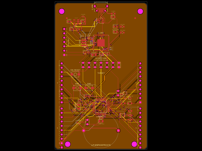 More from this authorShiboSoftwareDev/lp-msp430fr2476This design implements a microcontroller-based development board featuring an MSP430FR2476 target MCU with associated power regulation, USB host interface with ESD protection, multiple headers for peripherals and BoosterPacks, and integrated status LEDs and sensors.
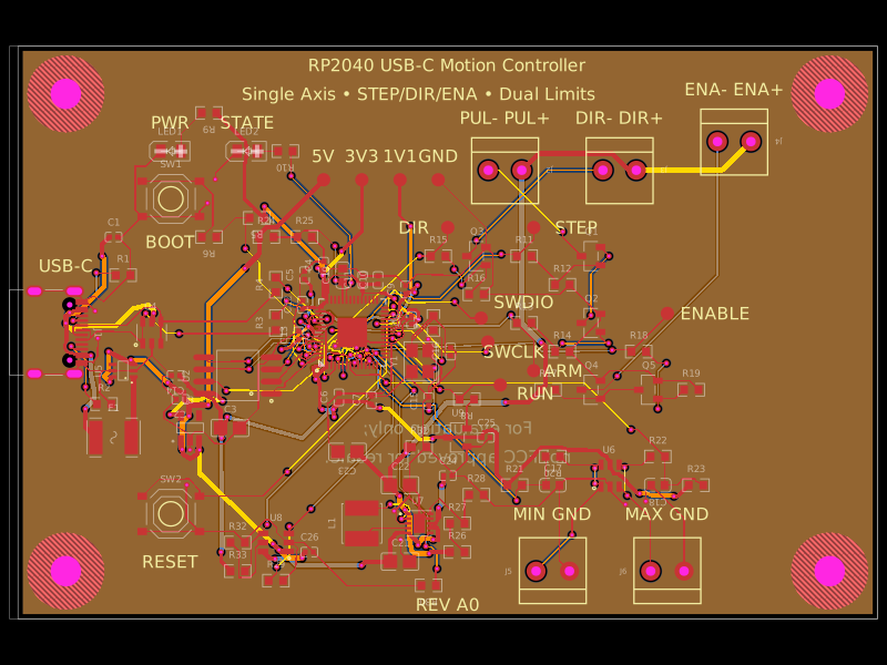 Similar packageAnasSarkiz/rp2040-usb-c-single-axis-dm542t-motion-controller--01a0e89cA USB‑C RP2040 controller board with external QSPI flash, crystal clock, regulated 3.3/1.1/5 V power, boost-converted motor-driver supply, protected USB and limit inputs, status LEDs, reset/boot switches, and AO3400A MOSFET outputs for stepper-control signals.
 Discover something newimrishabh18/fitness_watchThis circuit integrates an ESP-12E microcontroller with various sensors and peripherals, including a AO3400A MOSFET for switching loads, to enable wireless control and sensor data processing.