MustafaMulla29/rp2040-bldc-motor-controller-new
A tscircuit package created by MustafaMulla29.
- Version
- 0.3.101
- License
- unset
- Stars
- 0
imports/SI7111EDN_T1_GE3.tsx
// Vishay Si7111EDN: 30 V PMOS, RDS(on) <=16 mOhm at VGS=-2.5 V.
// PowerPAK 1212-8: S=1/2/3, G=4, D=5/6/7/8 and the exposed drain pad.
import { Fragment } from "react"
import type { ChipProps } from "@tscircuit/props"

const pinLabels = {
  pin1: ["S1"],
  pin2: ["S2"],
  pin3: ["S3"],
  pin4: ["G"],
  pin5: ["D4"],
  pin6: ["D3"],
  pin7: ["D2"],
  pin8: ["D1"]
} as const

// MOSFET gate is the control input; drain/source are passive switched terminals, not fixed supply pins.
const pinAttributes = {
  pin1: { isPassive: true },
  pin2: { isPassive: true },
  pin3: { isPassive: true },
  pin4: { isInput: true, mustBeConnected: true },
  pin5: { isPassive: true },
  pin6: { isPassive: true },
  pin7: { isPassive: true },
  pin8: { isPassive: true },
} as const

export const SI7111EDN_T1_GE3 = ({ sourceOnLeft = false, ...props }: ChipProps<typeof pinLabels> & { sourceOnLeft?: boolean }) => {
  // P-channel enhancement MOSFET, including its drain-to-source body diode.
  // All eight package pins stay distinct electrically. Parallel source/drain
  // pins share a schematic terminal, as in the manufacturer's circuit symbol.
  const mirror = sourceOnLeft ? -1 : 1
  const point = ({ x, y }: { x: number; y: number }) => ({ x: -y * mirror, y: x - 0.1 })
  const paths = [
    { points: [[0.02,0],[-0.1,-0.04],[-0.1,0.04],[0.02,0]], fill: true },
    { points: [[0.3,-0.04],[0.24,0.06],[0.36,0.06],[0.3,-0.04]], fill: true },
    { points: [[-0.1,0.14],[0.1,0.14],[0.1,0.2],[0.3,0.2],[0.3,0.06]] },
    { points: [[-0.1,0],[0.1,0],[0.1,-0.2],[0.3,-0.2],[0.3,-0.04]] },
    { points: [[0.1,-0.14],[-0.1,-0.14]] },
    { points: [[-0.14,0.18],[-0.14,-0.18]] },
    { points: [[-0.1,0.18],[-0.1,0.1]] },
    { points: [[-0.1,-0.04],[-0.1,0.04]] },
    { points: [[-0.1,-0.18],[-0.1,-0.1]] },
    { points: [[0.38,-0.04],[0.22,-0.04]] },
  ]
  return (
    <chip
      pinLabels={pinLabels}
      pinAttributes={pinAttributes}
      symbol={<symbol>
        <schematictext text="{NAME}" schX={0} schY={0.7} fontSize={0.18} anchor="center" />
        <schematictext text="SI7111EDN-T1-GE3" schX={0} schY={0.45} fontSize={0.13} anchor="center" />
        {paths.map((p, i) => <Fragment key={i}><schematicpath
          points={p.points.map(([x,y]) => point({x,y}))} strokeColor="#880000"
          isFilled={p.fill ?? false} fillColor="#880000" /></Fragment>)}
        {Object.entries(pinLabels).map(([name, aliases], i) => {
          const terminal = i < 3 ? {x:0.1,y:-0.4} : i === 3 ? {x:-0.3,y:0} : {x:0.1,y:0.4}
          const direction = i === 3 ? "down" : (i < 3) === (mirror === 1) ? "right" : "left"
          const p = point(terminal)
          return <Fragment key={name}><port name={aliases[0]} pinNumber={i + 1} aliases={[name]}
            direction={direction} schX={p.x} schY={p.y} schStemLength={i === 3 ? 0.16 : 0.2} /></Fragment>
        })}
      </symbol>}
      supplierPartNumbers={{
  "jlcpcb": [
    "C5690133"
  ]
}}
      manufacturerPartNumber="SI7111EDN-T1-GE3"
      footprint={<footprint>
        <smtpad portHints={["pin1"]} pcbX="-0.974979mm" pcbY="-1.434973mm" width="0.405003mm" height="0.9899904mm" shape="rect" />
<smtpad portHints={["pin2"]} pcbX="-0.324993mm" pcbY="-1.434973mm" width="0.405003mm" height="0.9899904mm" shape="rect" />
<smtpad portHints={["pin3"]} pcbX="0.324993mm" pcbY="-1.434973mm" width="0.405003mm" height="0.9899904mm" shape="rect" />
<smtpad portHints={["pin4"]} pcbX="0.974979mm" pcbY="-1.434973mm" width="0.405003mm" height="0.9899904mm" shape="rect" />
<smtpad portHints={["pin5"]} pcbX="0.974979mm" pcbY="1.434973mm" width="0.405003mm" height="0.9899904mm" shape="rect" solderPasteMargin={-2} />
<smtpad portHints={["pin6"]} pcbX="0.324993mm" pcbY="1.434973mm" width="0.405003mm" height="0.9899904mm" shape="rect" solderPasteMargin={-2} />
<smtpad portHints={["pin7"]} pcbX="-0.324993mm" pcbY="1.434973mm" width="0.405003mm" height="0.9899904mm" shape="rect" solderPasteMargin={-2} />
<smtpad portHints={["pin8"]} pcbX="-0.974979mm" pcbY="1.434973mm" width="0.405003mm" height="0.9899904mm" shape="rect" solderPasteMargin={-2} />
<smtpad portHints={["pin5"]} pcbX="0.000127mm" pcbY="0.557403mm" width="2.2349968mm" height="1.7249902mm" shape="rect" solderPasteMargin={-2} />
{/* Four exposed-drain windows plus four drain-finger apertures; factory stencil-process approval remains required. */}
{[-0.557373, 0.557627].flatMap(x => [0.127403, 0.987403].map(y => <solderpaste key={`${x}-${y}`} shape="rect" layer="top" pcbX={x} pcbY={y} width={1.0} height={0.73} />))}
{[-0.974979, -0.324993, 0.324993, 0.974979].map(x => <solderpaste key={`finger-${x}`} shape="rect" layer="top" pcbX={x} pcbY={1.675} width={0.305} height={0.41} />)}
<silkscreenpath route={[{"x":1.408658599999967,"y":1.6999458000000232},{"x":1.650034799999844,"y":1.6999458000000232}]} />
<silkscreenpath route={[{"x":-1.649983999999904,"y":1.6999458000000232},{"x":-1.408607800000027,"y":1.6999458000000232}]} />
<silkscreenpath route={[{"x":1.650034799999844,"y":-1.7000474000000168},{"x":1.650034799999844,"y":1.6999458000000232}]} />
<silkscreenpath route={[{"x":1.408658599999967,"y":-1.7000474000000168},{"x":1.650034799999844,"y":-1.7000474000000168}]} />
<silkscreenpath route={[{"x":-1.649983999999904,"y":-1.7000474000000168},{"x":-1.408607800000027,"y":-1.7000474000000168}]} />
<silkscreenpath route={[{"x":-1.649983999999904,"y":1.6999458000000232},{"x":-1.649983999999904,"y":-1.7000474000000168}]} />
<silkscreencircle pcbX="-1.410081mm" pcbY="-2.120011mm" radius="0.050038mm" />
<silkscreentext text="{NAME}" pcbX="-0.010287mm" pcbY="2.925193mm" anchorAlignment="center" fontSize="1mm" />
<courtyardoutline outline={[{"x":-1.8999586000001045,"y":2.1799681999998484},{"x":1.900034799999844,"y":2.1799681999998484},{"x":1.900034799999844,"y":-2.179968199999962},{"x":-1.8999586000001045,"y":-2.179968199999962},{"x":-1.8999586000001045,"y":2.1799681999998484}]} />
      </footprint>}
      cadModel={{
        objUrl: "https://modelcdn.tscircuit.com/easyeda_models/assets/C5690133.obj?uuid=83ddc30a76e5494dbc6c5642206c065a",
        stepUrl: "https://modelcdn.tscircuit.com/easyeda_models/assets/C5690133.step?uuid=83ddc30a76e5494dbc6c5642206c065a",
        pcbRotationOffset: 0,
        modelOriginPosition: { x: -0.000038099999983387534, y: 0.00006350000001020817, z: -0.02 },
      }}
      {...props}
      schRotation={0}
    />
  )
}
Related Packages
 More from this authorMustafaMulla29/MC-MP-symbolsThis code defines a 10mm x 10mm schematic diagram featuring two integrated circuit components ("MC" and "MP") with their respective physical symbols, including outer rings, lobed shapes, connection lines, and ports.
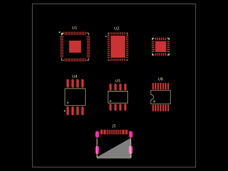 Similar packageAnasSarkiz/rp2040-bldc-servo-controllerRP2040-based motor-control board integrating a DRV8316 three-phase gate driver, AS5047P magnetic position sensor, USB-C power/communications, STUSB4500 USB-PD controller, SPI flash, and THVD1450 RS-485 transceiver.
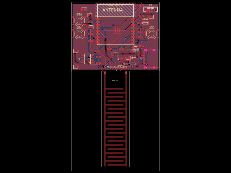 Discover something newgokul/musegrowUSB‑C powered ESP32‑C3 controller board with regulated 3.3 V supply, USB ESD protection, buttons/status LEDs, ambient-light I²C sensing, and a 555-driven capacitive soil-moisture electrode.