Ayushjhawar8/DRV8833-2X-Large
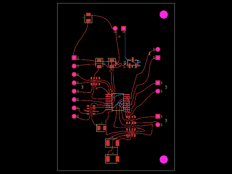
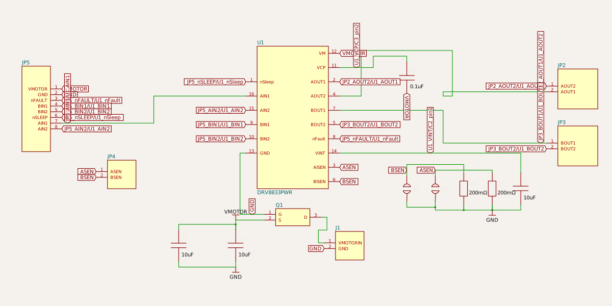
The code defines a PCB footprint and schematic representation for the DRV8833 motor driver IC, including its pin connections, supporting components, and physical layout.
- Version
- 1.0.0
- License
- unset
- Stars
- 0
index.tsx
PCB
Schematic
import { DRV8833PWR } from "./imports/DRV8833PWR"

export default function AdafruitDRV8833Breakout() {
  return (
    <board width="35.56mm" height="50.80mm" schAutoLayoutEnabled autorouter="auto_jumper">
      <chip
        name="JP5"
        footprint="pinrow8"
        pcbX={-12.7}
        pcbY={0}
        pcbRotation={270}
        schX={-9}
        schY={0.3}
        schWidth={1}
        schHeight={3}
        schPortArrangement={{
          rightSide: {
            pins: [1, 2, 3, 4, 5, 6, 7, 8],
            direction: "top-to-bottom",
          },
        }}
        pinLabels={{
          1: "VMOTOR",
          2: "GND",
          3: "nFAULT",
          4: "BIN1",
          5: "BIN2",
          6: "nSLEEP",
          7: "AIN1",
          8: "AIN2",
        }}
      />

      <chip
        name="JP2"
        footprint="pinrow2"
        pcbX={12.7}
        pcbY={-10.16}
        pcbRotation={270}
        schX={10}
        schY={1}
        schWidth={1.4}
        schHeight={1.4}
        schPortArrangement={{
          leftSide: {
            pins: [1, 2],
            direction: "top-to-bottom",
          },
        }}
        pinLabels={{
          1: "AOUT2",
          2: "AOUT1",
        }}
      />

      <chip
        name="JP3"
        footprint="pinrow2"
        pcbX={12.7}
        pcbY={0}
        pcbRotation={270}
        schX={10}
        schY={-1}
        schWidth={1.4}
        schHeight={1.4}
        schPortArrangement={{
          leftSide: {
            pins: [1, 2],
            direction: "top-to-bottom",
          },
        }}
        pinLabels={{
          1: "BOUT1",
          2: "BOUT2",
        }}
      />

      <chip
        name="JP4"
        footprint="pinrow2"
        pcbX={12.7}
        pcbY={10.16}
        pcbRotation={90}
        schX={-6}
        schY={-2}
        schWidth={1}
        schHeight={1}
        schPortArrangement={{
          leftSide: {
            pins: [1, 2],
            direction: "top-to-bottom",
          },
        }}
        pinLabels={{
          1: "ASEN",
          2: "BSEN",
        }}
      />

      <chip
        name="J1"
        footprint="pinrow2"
        pcbX={1.016}
        pcbY={17.78}
        pcbRotation={180}
        schX={2}
        schY={-4.5}
        schWidth={1}
        schHeight={1}
        schPortArrangement={{
          leftSide: {
            pins: [1, 2],
            direction: "top-to-bottom",
          },
        }}
        pinLabels={{
          1: "VMOTORIN",
          2: "GND",
        }}
      />

      <chip
        name="Q1"
        footprint="kicad:Package_TO_SOT_SMD/SOT-23"
        pcbX={5.08}
        pcbY={7.366}
        pcbRotation={90}
        schX={0}
        schY={-3.5}
        pinLabels={{
          1: "G",
          2: "S",
          3: "D",
        }}
      />

      <DRV8833PWR
        name="U1"
        pcbX={0.508}
        pcbY={-4.572}
        pcbRotation={90}
        schX={0}
        schY={0}
        schWidth={2.5}
        schHeight={5}
        schPinSpacing={0.5}
        schPortArrangement={{
          leftSide: {
            pins: [13, 10, 9, 15, 16, 1],
            direction: "bottom-to-top",
          },
          rightSide: {
            pins: [6, 3, 14, 8, 5, 7, 4, 2, 11, 12],
            direction: "bottom-to-top",
          },
        }}
      />

      <capacitor
        name="C1"
        capacitance="10uF"
        footprint="0805"
        pcbX={-8.382}
        pcbY={21.082}
        pcbRotation={90}
        schX={-4}
        schY={-4.5}
        schRotation={270}
      />
      <capacitor
        name="C4"
        capacitance="10uF"
        footprint="0805"
        pcbX={-1.27}
        pcbY={7.112}
        pcbRotation={270}
        schX={-2}
        schY={-4.5}
        schRotation={270}
      />

      <capacitor
        name="C2"
        capacitance="10uF"
        footprint="0805"
        pcbX={-4.318}
        pcbY={-12.446}
        pcbRotation={0}
        schX={8}
        schY={-2.5}
        schRotation={270}
      />

      <capacitor
        name="C3"
        capacitance="0.1uF"
        footprint="0805"
        pcbX={-5.08}
        pcbY={7.112}
        pcbRotation={270}
        schX={4}
        schY={1.4}
        schRotation={90}
      />

      <resistor
        name="R1"
        resistance="0.2ohm"
        footprint="1206"
        pcbX={-1.016}
        pcbY={-17.018}
        pcbRotation={0}
        schX={6}
        schY={-2.5}
        schRotation={270}
      />
      <resistor
        name="R2"
        resistance="0.2ohm"
        footprint="1206"
        pcbX={-1.016}
        pcbY={-21.844}
        pcbRotation={0}
        schX={7}
        schY={-2.5}
        schRotation={270}
      />

      <solderjumper name="SJ1" pcbX={-1.016} pcbY={-21.844} pcbRotation={180} schX={5} schY={-2.5} schRotation={270} />
      <solderjumper name="SJ2" pcbX={-1.016} pcbY={-17.018} pcbRotation={180} schX={4} schY={-2.5} schRotation={270} />

      <hole name="U$13" diameter={2.5} pcbX={14.48} pcbY={22} />
      <hole name="U$14" diameter={2.5} pcbX={14.48} pcbY={-22} />

      <trace from=".JP5 > .GND" to="net.GND" />
      <trace from=".J1 > .GND" to="net.GND" />
      <trace from=".U1 > .GND" to="net.GND" />
      <trace from=".Q1 > .G" to="net.GND" />
      <trace from=".C1 > .neg" to="net.GND" />
      <trace from=".C4 > .neg" to="net.GND" />
      <trace from=".C2 > .neg" to="net.GND" />
      <trace from=".R1 > .pin2" to="net.GND" />
      <trace from=".R2 > .pin2" to="net.GND" />
      <trace from=".SJ1 > .pin2" to="net.GND" />
      <trace from=".SJ2 > .pin2" to="net.GND" />

      <trace from=".U1 > .VM" to="net.VMOTOR" />
      <trace from=".JP5 > .VMOTOR" to="net.VMOTOR" />
      <trace from=".Q1 > .S" to="net.VMOTOR" />
      <trace from=".C1 > .pos" to="net.VMOTOR" />
      <trace from=".C4 > .pos" to="net.VMOTOR" />
      <trace from=".C3 > .pos" to="net.VMOTOR" />

      <trace from=".J1 > .VMOTORIN" to=".Q1 > .D" />

      <trace from=".U1 > .VCP" to=".C3 > .neg" />

      <trace from=".U1 > .VINT" to=".C2 > .pos" />

      <trace from=".JP5 > .AIN1" to=".U1 > .AIN1" />
      <trace from=".JP5 > .AIN2" to=".U1 > .AIN2" />
      <trace from=".JP5 > .BIN1" to=".U1 > .BIN1" />
      <trace from=".JP5 > .BIN2" to=".U1 > .BIN2" />
      <trace from=".JP5 > .nSLEEP" to=".U1 > .nSleep" />
      <trace from=".JP5 > .nFAULT" to=".U1 > .nFault" />

      <trace from=".JP2 > .AOUT2" to=".U1 > .AOUT1" />
      <trace from=".JP2 > .AOUT1" to=".U1 > .AOUT2" />
      <trace from=".JP3 > .BOUT1" to=".U1 > .BOUT1" />
      <trace from=".JP3 > .BOUT2" to=".U1 > .BOUT2" />

      <trace from=".U1 > .AISEN" to="net.ASEN" />
      <trace from=".U1 > .BISEN" to="net.BSEN" />

      <trace from=".R1 > .pin1" to="net.BSEN" />
      <trace from=".R2 > .pin1" to="net.ASEN" />

      <trace from=".SJ1 > .pin1" to="net.ASEN" />
      <trace from=".SJ2 > .pin1" to="net.BSEN" />

      <trace from=".JP4 > .ASEN" to="net.ASEN" />
      <trace from=".JP4 > .BSEN" to="net.BSEN" />
    </board>
  )
}
Related Packages
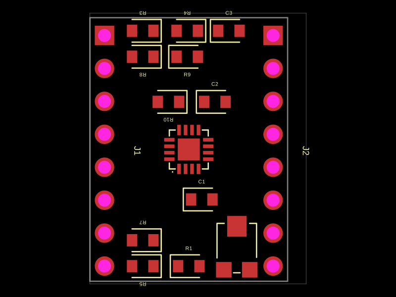 More from this authorAyushjhawar8/stepper-mini-motorThis code defines a schematic and PCB layout for a motor driver IC (TC78H670FTG) with associated passive components, power supply capacitors, resistors, headers, and mechanical footprints, all mapped with specific pin configurations and connections.
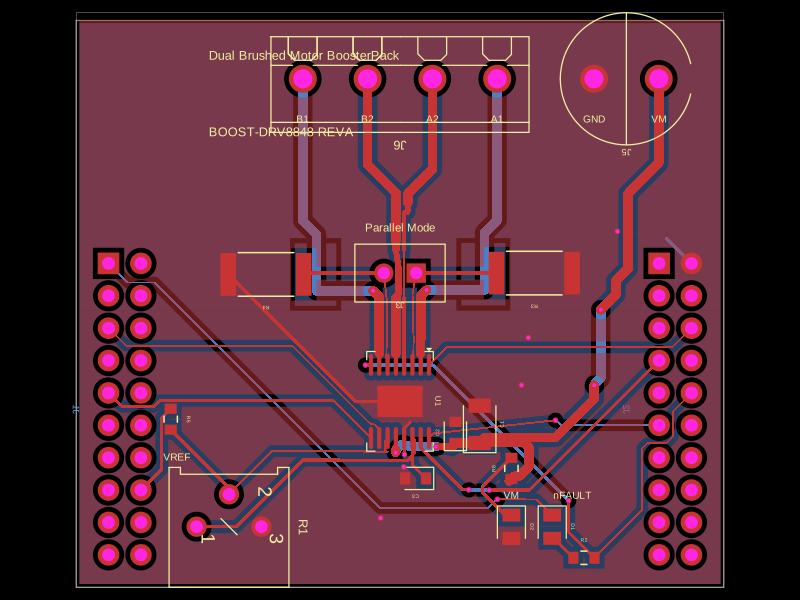 Similar packageMustafaMulla29/ti-boost-drv8848This code defines a hardware layout with 3D models, footprints, and schematic symbols for various electronic components including a potentiometer, motor driver ICs, connectors, capacitors, resistors, LEDs, and copper pours for ground overlays, assembled into a detailed schematic and PCB design.
 Discover something newimrishabh18/corne-keyboardA 3D-printed PLA enclosure for each Corne keyboard half, mounting the PCB with a base, plate, countersunk M3 fasteners, and optional switches/keycaps in exploded-view assembly.