AnasSarkiz/rp2040-bldc-servo-controller
RP2040-based motor-control board integrating a DRV8316 three-phase gate driver, AS5047P magnetic position sensor, USB-C power/communications, STUSB4500 USB-PD controller, SPI flash, and THVD1450 RS-485 transceiver.
- Version
- 0.0.5
- License
- unset
- Stars
- 0
POWER-REVIEW.md
# Preliminary power review - no finalized converter

Revision: intake-prototype-0.0.1, 2026-10-25. These are screening calculations, not circuit or hardware verification.

## Source evidence

- [Motor drawing A3122](https://files.omc-stepperonline.com/42BSA46-24-01.pdf): 24 V, rated 1.80 A, 25 W, 3000 rpm, 0.08 Nm, 2.74 ohm/phase +/-10%, 1.35 mH/phase +/-20%, 8 poles, Hall +5 V. Web-extracted text is available; PDF visual review and STEP access remain blocked.
- [STUSB4500 DS12499 Rev 8](https://www.st.com/resource/en/datasheet/stusb4500.pdf): up to 20 V / 5 A, three sink PDOs; not a 24 V power source.
- [ST UM2650 Rev 3](https://www.st.com/resource/en/user_manual/um2650-the-stusb4500-software-programing-guide-stmicroelectronics.pdf): contract/RDO and source-capability handling, PDO updates and renegotiation.
- [DRV8316 SLVSF16B](https://www.ti.com/lit/ds/symlink/drv8316.pdf) and [DRV8316xEVM SLVUBZ9B](https://www.ti.com/lit/ug/slvubz9b/slvubz9b.pdf): integrated FETs and current sensing; 4.5-35 V operating range, 40 V absolute maximum. The 8 A peak headline is not a guaranteed continuous-current board rating.
- [LM5122EVM SNVU197](https://www.ti.com/lit/ug/snvu197/snvu197.pdf): manufacturer reference design for 9-20 V input and 24 V / 4.5 A output; its reported efficiency and load-step behavior apply to that EVM, not this board. It needs more than 100 W input at full output, so it cannot simply be copied without contract-aware derating.
- [LM5122 SNVS954H](https://www.ti.com/lit/ds/symlink/lm5122.pdf): candidate synchronous boost controller, external power switches, programmable peak current limit, soft-start and hiccup protection. This is not yet a qualified design.

## Power envelopes

25 W is not a safe assumption for electrical supply demand: at the stated torque and speed, mechanical shaft power is 0.08 * 3000 * 2*pi/60 = 25.13 W. The rated voltage/current product is 24 * 1.8 = 43.2 W. The definition of rated current and actual phase waveform must be established before converting that number into a FOC phase-current limit.

| Screening case | Calculation | Result |
| --- | --- | --- |
| Maximum nominal PD source contract | 20 V * 5 A | 100 W at source, before cable/path losses |
| Rated voltage/current product | 24 V * 1.8 A | 43.2 W, not proof of peak demand |
| Illustrative 24 V / 3 A bus target | 24 * 3 | 72 W |
| Illustrative input with 90% boost and 2 W other loads | 72/0.90 + 2 | 82 W, 4.10 A at 20 V |
| Same demand at illustrative 19 V board input | 82/19 | 4.32 A |
| Illustrative boost heat at 72 W, 90% | 72*(1/0.90 - 1) | 8 W; substantial on a motor-sized board |
| Ideal 20 -> 24 V boost duty | 1 - 20/24 | 16.7% |
| Ideal 15 -> 24 V boost duty | 1 - 15/24 | 37.5% |
| Ideal 9 -> 24 V boost duty | 1 - 9/24 | 62.5% |
| Ideal 5 -> 24 V boost duty | 1 - 5/24 | 79.2% |

The 90% efficiency, 19 V input, 2 W overhead and 3 A output are explicitly illustrative assumptions. No part selection, loss model, operating-temperature budget or source contract proves them. Full motor power must not be enabled at 5/9/15 V on the strength of these calculations. Lower contracts should keep the motor disabled until a separately verified derating policy exists.

For an example 20 V, 100 W source with 2 W reserved for logic and 90% boost efficiency, the ideal remaining 24 V output ceiling is (100-2)*0.9/24 = 3.675 A before cable losses, current-limit tolerances and thermal derating. It is not a proposed allowable motor current. Startup, load steps and a locked rotor require active limits rather than an assumption that 100 W is sufficient.

## Required unresolved verification

1. Define phase RMS/peak current, startup acceleration, arm inertia, gearing, maximum sustained torque, motion duty and fault response. Prove power and phase-current limits independently; a DC bus current limit alone does not cap recirculating phase current.
2. Select and import every boost/protection component. Calculate inductor ripple and saturation at maximum temperature and minimum input, MOSFET/diode stress and switching loss, sense threshold tolerances, capacitor bias/ripple current and loop stability. Verify startup into actual load and output capacitance, load dump and repeated hiccup.
3. Prevent boost inrush and body-diode feedthrough from violating the active USB contract. Provide output short-circuit disconnection and reverse-current blocking where required; controller shutdown alone is insufficient.
4. Establish independent undervoltage/overvoltage and thermal interlocks and measure their tolerances/response. Sequence DRV8316 nFAULT pullup correctly: TI warns that below 2.2 V at startup can enter test mode. Assert DRVOFF and nSLEEP default states reliably during all rail transitions.
5. Implement local regenerative-energy handling. Capacitor-only storage obeys E = 0.5*C*(V_high^2 - V_low^2). For illustration, 1 mF from 24 V to 28 V stores only 0.104 J; this is not an approved bus clamp voltage or actual capacitor selection. Arm energy is unknown, so a brake resistor/chopper and thermal budget cannot be sized yet.
6. Validate USB host programming/communications at initial 5 V with the motor disabled. A power-only PD brick supplies no USB host function; firmware loading requires a data-capable host/cable arrangement.

**Outcome:** USB-C-only operation is the requirement. The preliminary budget does not prove a boost converter can meet startup/transient demand or fit thermally on the exact motor rear face. Power qualification remains blocked, not passed.

## 2026-10-26 screening follow-up — prototype 0.0.3

This section extends the earlier review. It does not select or implement a converter and does not depend on a motor mounting assumption.

### Candidate screening and manufacturer evidence

- [TPS55288 SLVSF01B](https://www.ti.com/lit/ds/symlink/tps55288.pdf), archived as `datasheets/tps55288.pdf`: **rejected for the regulated 24 V motor bus**. The output range ends at 22 V. The 36 V headline describes input tolerance; neither the input rating nor 16 A internal-switch rating authorizes 24 V output. Page 6 was rendered and its output-limit table visually reviewed.
- [TPS55340 SLVSBD4E](https://www.ti.com/lit/ds/symlink/tps55340.pdf), archived as `datasheets/tps55340.pdf`: screened for possible 20-to-24 V conversion. Input 2.9–32 V, boost output up to 38 V, internal switch absolute maximum 40 V. Table 6.5 gives internal switch current limit 5.25 A minimum, 6.6 A typical and 7.75 A maximum. Those are **switch-current limits**, not guaranteed output-current ratings. QFN junction-to-ambient 43.3 °C/W is a reference-board thermal metric, not a motor-mounted PCB thermal guarantee. Pages 3 and 5 were rendered and visually reviewed; application section 8.2.1 equations were consulted. Complete component/reference-layout qualification remains unfinished.
- The official JLCPCB listing identifies TPS55340RTER as **C169167**, WQFN-16-EP(3x3), Extended, stock 18,223, available order quantity 18,106 on 2026-10-26. Exact import succeeds, but table 5-1 requires NC pins 10/14 grounded whereas the imported metadata forbids connecting them. This **blocks dependent converter implementation** under I-018. It is a screening candidate only; no manual metadata changes are made.
- LM5122 remains the earlier alternative candidate. The family-name searches for TPS55340 and LM5122 returned unrelated parts; the real TPS55340 supplier code was obtained from the official assembler listing, then exact-ID searched and imported. No unrelated search result was treated as a substitute.

### Contract-aware analytical envelope

Reproduce with `python3 scripts/power-envelope.py`; full inputs and nine operating points are in `evidence/tooling-20261026/power-envelope.json`. The following are **screening assumptions**, not selected-component or measured limits: 90% boost efficiency, 2 W other loads, nominal input current limit 4.5 A ±5%, board input 18–20 V, nominal 10 µH inductor at −20% tolerance (8 µH), and 0.5 V diode drop. The 460 kHz frequency used for ripple screening is the datasheet minimum at RFREQ = 80 kΩ; no actual resistor or its tolerance has been selected. The input range is a hypothetical board operating envelope, not an asserted USB PD cable-drop guarantee.

The assumed limiter spans **4.275–4.725 A**. The upper bound stays below the required negotiated 5 A, while the lower bound controls guaranteed available power. Both other-load power and boost losses must be included:

`I_input = (24 × I_bus / efficiency + P_other) / V_board`

`I_bus_available = (V_board × I_limit_min − P_other) × efficiency / 24`

| Screening point | Result under these assumptions |
| --- | --- |
| 18 V board input, 24 V / 2 A bus | Fits the assumed current budget and switch-current screen; this is not a tested continuous rating. |
| 18 V board input, 24 V / 3 A bus | Needs 4.556 A input, above the 4.275 A lower current-limit bound; fails the power-budget screen. |
| Maximum bus current at 18 V under the assumed limiter/efficiency | 2.811 A at 24 V before further derating. |
| Minimum board input for 24 V / 3 A under those assumptions | 19.181 V. A nominal 20 V contract alone does not establish that voltage at the PCB. |
| 1 A load step lasting 500 µs, allowing 0.5 V capacitive sag | 1,000 µF **effective** capacitance, before ESR/ESL and control-loop response. No capacitor is selected by this illustrative calculation. |
| 1 mF capacitor absorbing energy from 24 V to 28 V | 0.104 J; unchanged reason that an unknown arm braking load cannot be covered by an assumed capacitor. |

Inductor ripple and peak current are screened separately using continuous-conduction first-order equations. The model omits detailed switch/diode waveforms, parasitics, loop response, losses versus temperature and input-filter dynamics. Saturation/fault sizing must consider the **maximum** internal current limit (7.75 A plus relevant overshoot), not just the minimum limit used for output capability. Input capacitors can supply switching peaks above the upstream averaged current limit.

TPS55340's diode/inductor path can feed the output even when switching is disabled. Output short protection, controlled precharge/inrush, reverse-feed prevention, independent voltage/temperature interlocks, braking energy dissipation and hardware motor-disable remain mandatory and undesigned. Motor phase current cannot be inferred from this DC bus-current calculation.

Only a verified adequate **20 V / 5 A** contract may enable the proposed full-power motor path. Initial attachment and 5/9/15 V or insufficient-current contracts keep it disabled. The four requested voltage choices still need a documented STUSB4500 three-PDO reconfiguration strategy. Booting logic from initial 5 V must not accidentally turn on the boost/motor path.

**Startup/transient capability remains unverified.** The actual motor current definition, acceleration, arm inertia, duty, regenerated energy, effective capacitance, compensation, thermal model and prototype measurements are still missing. No 2 A continuous or 3 A surge hardware rating is claimed from these screening results.
Related Packages
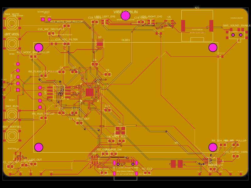 More from this authorAnasSarkiz/vibe_GoblinThese code snippets define various physical electronic components such as ICs, connectors, sensors, LEDs, and chips, specifying their pin layouts, footprint pads, silkscreen markings, courtyard outlines, and 3D CAD models for placement on PCB boards.
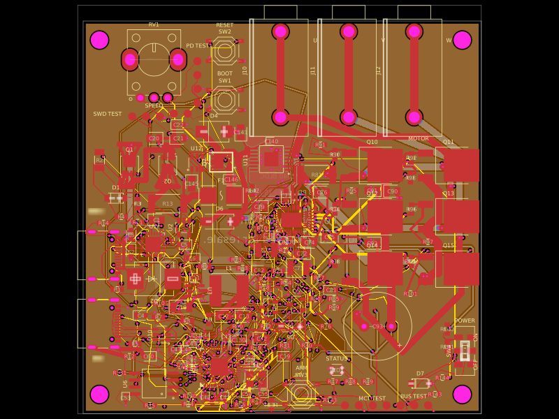 Similar packageMustafaMulla29/rp2040-bldc-motor-controller-new73×72 mm 4-layer USB‑C PD (5/9/15/20 V) RP2040 controller PCB with protected power switching, MCT8329A sensorless BLDC three-phase MOSFET bridge, USB data/programming, onboard controls, and three motor outputs feeding a 2212 motor through rigid bullet adapters.
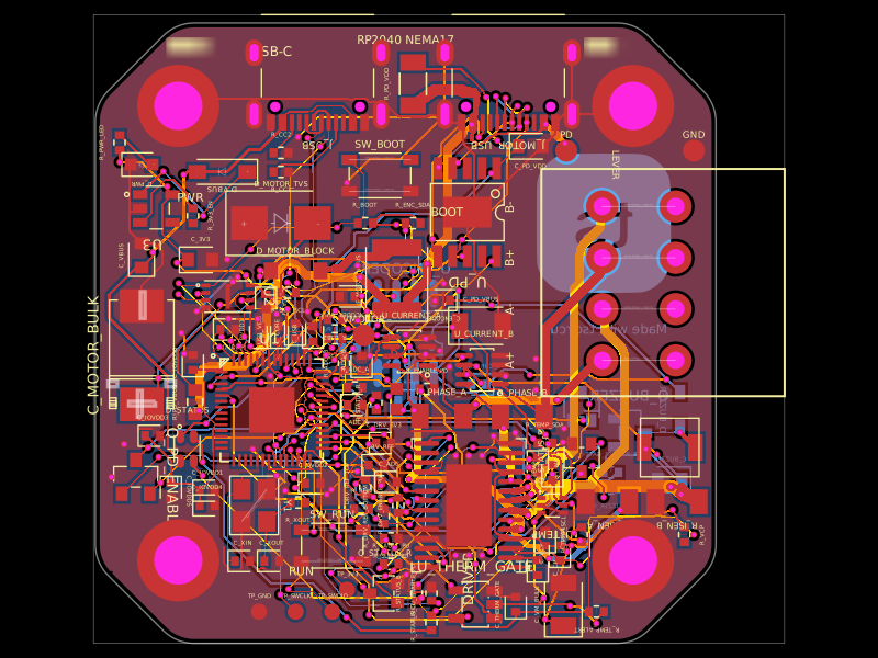 Discover something newastra/nema17-stepper-motor-controller-spring-clamp-rp2040A 4-layer RP2040 controller board that negotiates USB‑C PD motor power and drives a NEMA17 stepper via a DRV8825, with current sensing, thermal shutdown, RGB status LED, buzzer alarm, optional AS5600 encoder, protection/filtering, and test points.