AnasSarkiz/rp2040-bldc-servo-controller
RP2040-based motor-control board integrating a DRV8316 three-phase gate driver, AS5047P magnetic position sensor, USB-C power/communications, STUSB4500 USB-PD controller, SPI flash, and THVD1450 RS-485 transceiver.
- Version
- 0.0.5
- License
- unset
- Stars
- 0
PIN-REVIEW.md
# Pin review and proposed allocation - no implemented wiring

2026-10-25, intake-prototype-0.0.1. Imported definitions are kept unchanged. This record is not a complete electrical review.

## DRV8316R

Checked against SLVSF16B table 6-1: VM 9/10/11; PGND 12/15/18; AGND 2/26; exposed pad 41; U 13/14; V 16/17; W 19/20; DRVOFF 21; nFAULT 22; nSLEEP 23; AVDD 25; INHA/INLA 27/28; INHB/INLB 29/30; INHC/INLC 31/32; SDO 33; SDI 34; SCLK 35; nSCS 36; VREF/ILIM 37; SOC/SOB/SOA 38/39/40; NC 1/24; buck FB/GND/SW 3/4/5; CPL/CPH/CP 6/7/8.

SOA/B/C are integrated current-sense outputs, not external shunt inputs. Their valid PWM sampling windows, offset, gain and settling must be designed with the RP2040 ADC's sequential sampling. TI requires charge-pump and rail decoupling, including 47 nF CPH-CPL and 1 uF CP-VM. The exact imported support capacitors have not been selected. Default OCP does not establish a 1.8 A motor-current limit. nFAULT and SDO require pullups, with the startup condition described in POWER-REVIEW.md.

## RP2040 dedicated pins

QSPI SS 56; SD1 55; SD2 54; SD0 53; SCLK 52; SD3 51. USB D+ 47, D- 46, USB_VDD 48. Internal regulator input 44/output 45. ADC_AVDD 43. DVDD 23/50. IOVDD 1/10/22/33/42/49. XIN/XOUT 20/21. TESTEN 19 must be grounded. SWCLK 24, SWDIO 25, RUN 26, exposed GND 57. The complete regulator, clock, decoupling, BOOTSEL/reset, USB termination/protection and SWD circuits remain unimplemented.

## Proposed GPIO assignment for subsequent electrical review

| RP2040 GPIO | Proposed function | Peripheral |
| --- | --- | --- |
| 0 / 1 / 2 / 3 / 4 / 5 | INHA/INLA/INHB/INLB/INHC/INLC | PWM slices 0/1/2 A/B |
| 6 / 7 | STUSB4500 SDA / SCL | I2C1 |
| 8 / 9 | RS-485 TX / RX | UART1 |
| 10 | RS-485 DE and /RE control | GPIO |
| 11 / 12 | Driver nFAULT / nSLEEP | GPIO |
| 13 | Hardware-interlock arm request | GPIO |
| 14 / 15 / 21 | Hall A/B/C via protected 3.3 V inputs | GPIO/PIO |
| 16 / 18 / 19 | Shared driver/encoder MISO / SCLK / MOSI | SPI0 |
| 17 / 20 | Driver / encoder chip selects | GPIO |
| 22 | PD ALERT | GPIO |
| 23 / 24 / 25 | Reserved for PD reset, watchdog and fault monitoring | GPIO, allocation not final |
| 26 / 27 / 28 | Current SOA/SOB/SOC after RC filters | ADC0/1/2 |
| 29 | Motor bus voltage via rated divider/filter | ADC3 |

The shared SPI bus needs verified device modes, clock limits, deselected output behavior and separate chip selects. This avoids claiming that alternate SPI0 pin groups are independent controllers. Hardware protection status and temperature sensing may need an I2C monitor; exact components and pin commitments remain unresolved. Firmware must synchronize PWM slices, impose dead time as required by the driver, align ADC sampling, and verify worst-case control deadlines; none has been tested.

## USB-C and encoder

USB4215 import uses logical pins 17/28 for combined GND contacts, 18/27 for combined VBUS contacts, 20/26 CC1/CC2, 22/24 D+ and 21/23 D-, 19/25 SBU2/SBU1 and 13-16 shell stakes. Manufacturer contact names are also imported as aliases. Both orientations require USB 2.0 continuity; SBU is unused. Connector shell bonding and rated pad/slot geometry require visual review.

AS5047P import: CSn 1, CLK 2, MISO 3, MOSI 4, TEST 5, B 6, A 7, W/PWM 8, V 9, U 10, VDD 11, VDD3V3 12, GND 13, I 14. The current Infineon-hosted manufacturer datasheet was located and its pin table checked through the web PDF reader; the local download returned an empty body. TEST must connect to ground, inputs must not float, and in 3.3 V mode VDD and VDD3V3 must be tied together with the specified local decoupling. Complete electrical review remains open. Mechanical magnet placement and the external daughterboard are unvalidated.
Related Packages
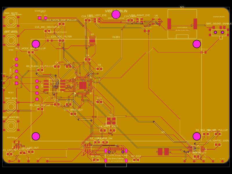 More from this authorAnasSarkiz/vibe_GoblinThese code snippets define various physical electronic components such as ICs, connectors, sensors, LEDs, and chips, specifying their pin layouts, footprint pads, silkscreen markings, courtyard outlines, and 3D CAD models for placement on PCB boards.
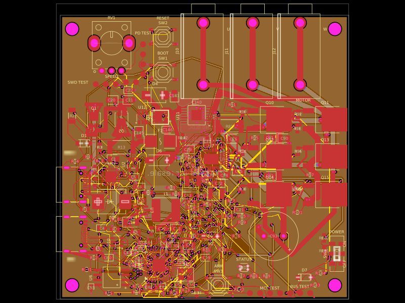 Similar packageMustafaMulla29/rp2040-bldc-motor-controller-new73×72 mm 4-layer USB‑C PD (5/9/15/20 V) RP2040 controller PCB with protected power switching, MCT8329A sensorless BLDC three-phase MOSFET bridge, USB data/programming, onboard controls, and three motor outputs feeding a 2212 motor through rigid bullet adapters.
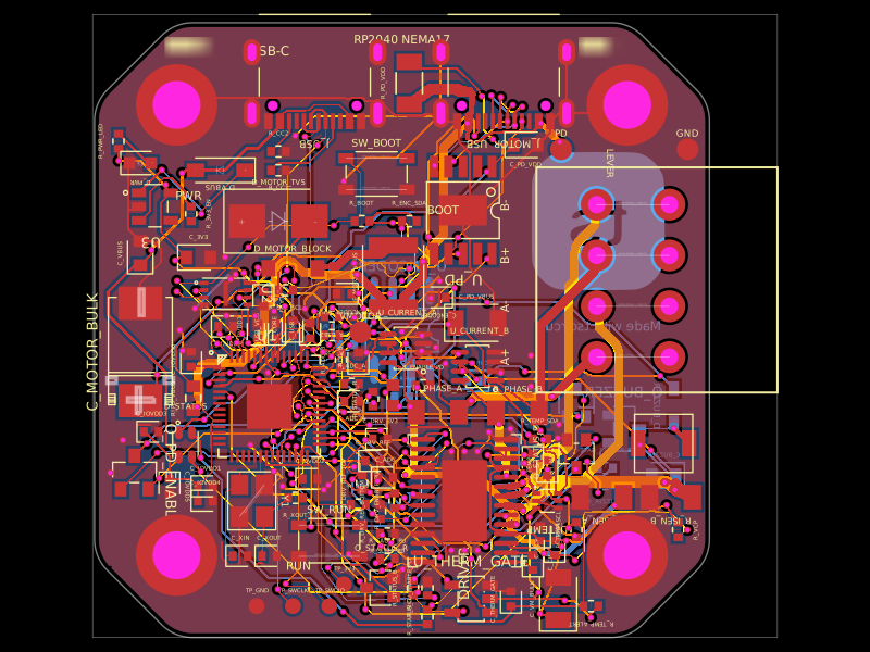 Discover something newastra/nema17-stepper-motor-controller-spring-clamp-rp2040A 4-layer RP2040 controller board that negotiates USB‑C PD motor power and drives a NEMA17 stepper via a DRV8825, with current sensing, thermal shutdown, RGB status LED, buzzer alarm, optional AS5600 encoder, protection/filtering, and test points.