AnasSarkiz/muse-voice-remote
Muse Voice Remote — bare ESP32-S3R8, 155 TOP JLCPCB parts with real supplier CAD, native 3D assembly and GLB exports. Revised 17 mm case allocation; 0.30 mm via drill /0.45 mm pad. Checked prototype PCB; mechanical, RF and MUSE qualification pending.
- Version
- 1.3.2
- License
- unset
- Stars
- 0
vendor/jlcpcb/library/C221665.kicad_mod
(module easyeda2kicad:SW-SMD_JS202011JCQN (layer F.Cu) (tedit 5DC5F6A4)
	(attr smd)
	(fp_text reference REF** (at 0.000 -5.200) (layer F.SilkS)
		(effects (font (size 1 1) (thickness 0.15)))
	)
	(fp_text value SW-SMD_JS202011JCQN (at 0.000 5.200) (layer F.Fab)
		(effects (font (size 1 1) (thickness 0.15)))
	)
	(fp_text user %R (at 0 0) (layer F.Fab)
		(effects (font (size 1 1) (thickness 0.15)))
	)
	(property "LCSC Part" "C221665")
	(fp_line (start -4.50 1.75) (end -4.50 -1.75) (layer F.SilkS) (width 0.25))
	(fp_line (start 4.50 -1.75) (end 4.50 1.75) (layer F.SilkS) (width 0.25))
	(fp_line (start -4.50 -1.75) (end -3.27 -1.75) (layer F.SilkS) (width 0.25))
	(fp_line (start -1.81 -1.75) (end -0.73 -1.75) (layer F.SilkS) (width 0.25))
	(fp_line (start 0.73 -1.75) (end 1.81 -1.75) (layer F.SilkS) (width 0.25))
	(fp_line (start 3.27 -1.75) (end 4.50 -1.75) (layer F.SilkS) (width 0.25))
	(fp_line (start -4.50 1.75) (end -3.27 1.75) (layer F.SilkS) (width 0.25))
	(fp_line (start -1.81 1.75) (end -0.73 1.75) (layer F.SilkS) (width 0.25))
	(fp_line (start 0.73 1.75) (end 1.81 1.75) (layer F.SilkS) (width 0.25))
	(fp_line (start 3.27 1.75) (end 4.50 1.75) (layer F.SilkS) (width 0.25))
	(fp_line (start -1.78 0.76) (end -0.73 0.76) (layer F.SilkS) (width 0.25))
	(fp_line (start 0.73 0.76) (end 1.78 0.76) (layer F.SilkS) (width 0.25))
	(fp_line (start -1.78 -0.76) (end -0.73 -0.76) (layer F.SilkS) (width 0.25))
	(fp_line (start 0.73 -0.76) (end 1.78 -0.76) (layer F.SilkS) (width 0.25))
	(fp_line (start -1.78 -0.76) (end -1.78 0.76) (layer F.SilkS) (width 0.25))
	(fp_line (start 1.78 -0.76) (end 1.78 0.76) (layer F.SilkS) (width 0.25))
	(fp_line (start 0.51 -0.17) (end 0.51 0.17) (layer F.SilkS) (width 0.25))
	(fp_line (start -0.51 -0.17) (end -0.51 0.17) (layer F.SilkS) (width 0.25))
	(fp_line (start -1.52 0.51) (end -0.73 0.51) (layer F.SilkS) (width 0.25))
	(fp_line (start -1.52 0.51) (end -1.52 -0.51) (layer F.SilkS) (width 0.25))
	(fp_line (start -1.52 -0.51) (end -0.73 -0.51) (layer F.SilkS) (width 0.25))
	(fp_line (start 1.02 -0.51) (end 0.73 -0.51) (layer F.SilkS) (width 0.25))
	(fp_line (start 1.02 -0.51) (end 1.02 0.51) (layer F.SilkS) (width 0.25))
	(fp_line (start 1.02 0.51) (end 0.73 0.51) (layer F.SilkS) (width 0.25))
	(pad 1 smd rect (at -2.54 -1.20 0.00) (size 1.000 1.600) (layers F.Cu F.Paste F.Mask))
	(pad 2 smd rect (at 0.00 -1.20 0.00) (size 1.000 1.600) (layers F.Cu F.Paste F.Mask))
	(pad 3 smd rect (at 2.54 -1.20 0.00) (size 1.000 1.600) (layers F.Cu F.Paste F.Mask))
	(pad 5 smd rect (at -2.54 1.20 0.00) (size 1.000 1.600) (layers F.Cu F.Paste F.Mask))
	(pad 6 smd rect (at 0.00 1.20 0.00) (size 1.000 1.600) (layers F.Cu F.Paste F.Mask))
	(pad 7 smd rect (at 2.54 1.20 0.00) (size 1.000 1.600) (layers F.Cu F.Paste F.Mask))
	(fp_circle (center -4.50 -1.80) (end -4.47 -1.80) (layer F.SilkS) (width 0.06))
	(fp_line (start -4.50 1.80) (end -4.50 -1.80) (layer F.CrtYd) (width 0.05))
	(fp_line (start -4.50 -1.80) (end 4.50 -1.80) (layer F.CrtYd) (width 0.05))
	(fp_line (start 4.50 -1.80) (end 4.50 1.80) (layer F.CrtYd) (width 0.05))
	(fp_line (start 4.50 1.80) (end -4.50 1.80) (layer F.CrtYd) (width 0.05))
	(model "/SW-SMD_JS202011JCQN.wrl"
		(offset (xyz 0.000 0.000 0.000))
		(scale (xyz 1 1 1))
		(rotate (xyz 0 0 0))
	)
)
Related Packages
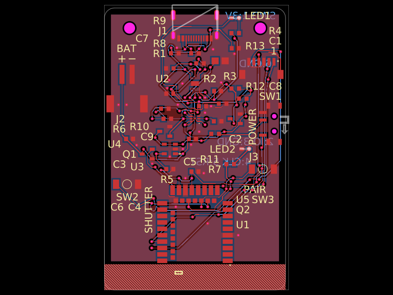 More from this authorAnasSarkiz/magnetic-shutter-remote--01a0f81fA compact USB‑C rechargeable battery device with BQ25185 charging, 3.3‑V regulation and protection, E73 Bluetooth control, temperature monitoring, status/charge LEDs, shutter/pair/power switches, and a mechanically enclosed Li‑Po battery with docking/antenna provisions.
 Similar packagemohan-bee/esp32-c3This hardware design integrates an ESP32-C3 microcontroller, a USB-C connector, a power management IC (AP2112-3.3V regulator), a USB-to-Serial converter (CH340C), several resistors, capacitors, and user-accessible headers to facilitate USB communication, power regulation, and general I/O interfacing.
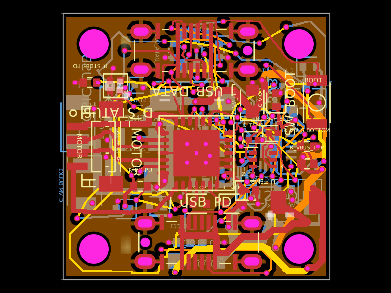 Discover something newShiboSoftwareDev/nema8-20mm-dual-usbc-stepper-controllerA compact 20 mm four-layer USB‑C stepper-controller PCB combining CH32X035 MCU control, TMC2209 motor driving, USB‑C PD/data interfaces, protection/power regulation, temperature/LED status hardware, and NEMA8 motor connectivity.