AnasSarkiz/muse-voice-remote
Muse Voice Remote — bare ESP32-S3R8, 155 TOP JLCPCB parts with real supplier CAD, native 3D assembly and GLB exports. Revised 17 mm case allocation; 0.30 mm via drill /0.45 mm pad. Checked prototype PCB; mechanical, RF and MUSE qualification pending.
- Version
- 1.3.2
- License
- unset
- Stars
- 0
vendor/espressif-bare-s3/schematic-checklist.rst
Schematic Checklist
======================
:link_to_translation:`zh_CN:[中文]`

.. _schematic-checklist-overview:

Overview
---------

{IDF_TARGET_ELEC_COMP_NUM: default="20", esp32h2="17", esp32c2="15", esp32c5="30", esp32c61="30", esp32s31="30"}

{IDF_TARGET_ELEC_COMP: default=", as well as an SPI flash", esp32c6=", as well as an SPI flash (not needed for QFN32 package)", esp32h2="", esp32c2="", esp32c61=", as well as an SPI flash (in-package or off-package)"}

The integrated circuitry of {IDF_TARGET_NAME} requires only {IDF_TARGET_ELEC_COMP_NUM} electrical components (resistors, capacitors, and inductors) and a crystal{IDF_TARGET_ELEC_COMP}. The high integration of {IDF_TARGET_NAME} allows for simple peripheral circuit design. This chapter details the schematic design of {IDF_TARGET_NAME}.

The following figure shows a reference schematic design of {IDF_TARGET_NAME}. It can be used as the basis of your schematic design.

.. only:: esp32s31

    .. note::

        The core circuit is the minimum required circuit. Please do not remove components arbitrarily.

.. only:: not esp32c6

    .. figure:: ../_static/{IDF_TARGET_PATH_NAME}/{IDF_TARGET_PATH_NAME}-sche-core.png
        :name: fig-chip-core-schematic
        :align: center
        :width: 95%
        :alt: {IDF_TARGET_NAME} Reference Schematic

        {IDF_TARGET_NAME} Reference Schematic

.. only:: esp32c6

    .. figure:: ../_static/{IDF_TARGET_PATH_NAME}/{IDF_TARGET_PATH_NAME}-sche-core-qfn40.png
        :name: fig-chip-core-schematic
        :align: center
        :width: 95%
        :alt: {IDF_TARGET_NAME} Reference Schematic for QFN40 Package

        {IDF_TARGET_NAME} Reference Schematic for QFN40 Package

    .. figure:: ../_static/{IDF_TARGET_PATH_NAME}/{IDF_TARGET_PATH_NAME}-sche-core-qfn32.png
        :name: fig-chip-core-schematic-qfn32
        :align: center
        :width: 95%
        :alt: {IDF_TARGET_NAME} Reference Schematic for QFN32 Package

        {IDF_TARGET_NAME} Reference Schematic for QFN32 Package

.. only:: esp32 or esp32s3 or esp32c6 or esp32c2

    .. include:: {IDF_TARGET_PATH_NAME}/{IDF_TARGET_PATH_NAME}-chip-core-schem-note.inc

Any basic {IDF_TARGET_NAME} circuit design may be broken down into the following major building blocks:

.. list::

    - `Power supply`_
    - `Chip power-up and reset timing`_
    :esp32h2 or esp32c3 or esp32c6 or esp32c2: - `Flash`_
    :esp32 or esp32s2 or esp32s3 or esp32c5 or esp32c61 or esp32s31: - `Flash and PSRAM`_
    - `Clock source`_
    - `RF`_
    - `UART`_
    - `SPI`_
    - `Strapping pins`_
    :esp32 or esp32s31: - `External capacitor`_
    - `GPIO`_
    - `ADC`_
    :esp32 or esp32s3 or esp32c6 or esp32c5 or esp32c61: - `SDIO`_
    :esp32s31: - `SD/MMC Host Controller`_
    :esp32h2 or esp32s2 or esp32s3 or esp32c6 or esp32c3 or esp32c5 or esp32c61 or esp32s31: - `USB`_
    :esp32 or esp32s2 or esp32s3 or esp32s31: - `Touch sensor`_
    :esp32s31: - `Ethernet MAC`_
    :esp32s31: - `LCD and Camera Controller`_

The rest of this chapter details the specifics of circuit design for each of these sections.

.. _schematic-checklist-power-supply:

Power Supply
----------------

{IDF_TARGET_OUTPUT_CUR:default="500 mA", esp32h2="350 mA", esp32c5="600 mA", esp32s31="600 mA"}

The general recommendations for power supply design are:

- When using a single power supply, the recommended power supply voltage is 3.3 V and the output current is no less than {IDF_TARGET_OUTPUT_CUR}.
- It is suggested to add an ESD protection diode and at least 10 μF capacitor at the main power entrance (where the external power supply enters the PCB).

.. only:: not esp32c5 and not esp32s3 and not esp32 and not esp32c61 and not esp32c6 and not esp32s31

    The power scheme is shown in `{IDF_TARGET_NAME} Series Datasheet <{IDF_TARGET_DATASHEET_EN_URL}#cd-pwr-scheme>`__ > Figure *{IDF_TARGET_NAME} Power Scheme*.

.. only:: esp32c5 or esp32s3 or esp32 or esp32c6 or esp32s31

    The power scheme is shown in Figure :ref:`fig-chip-power-scheme`.

    .. figure:: ../_static/{IDF_TARGET_PATH_NAME}/{IDF_TARGET_PATH_NAME}-sche-chip-power.png
       :name: fig-chip-power-scheme
       :align: center
       :width: 100%
       :alt: {IDF_TARGET_NAME} Power Scheme

       {IDF_TARGET_NAME} Power Scheme

More information about power supply pins can be found in `{IDF_TARGET_NAME} Series Datasheet <{IDF_TARGET_DATASHEET_EN_URL}#cd-pwr-supply>`__ > Section *Power Supply*.

.. _digital-power-supply:

Digital Power Supply
^^^^^^^^^^^^^^^^^^^^^^^^

{IDF_TARGET_DIG_POWER_PIN:default="pin17 VDD3P3_CPU", esp32="pin37 VDD3P3_CPU", esp32s2="pin27 VDD3P3_RTC_IO and pin45 VDD3P3_CPU", esp32s3="pin46 VDD3P3_CPU", esp32c6="pin5 VDDPST1 and pin28 VDDPST2", esp32h2="pin9 VDDPST1 and pin20 VDDPST2", esp32c5="VDDPST1 (pin8), VDDPST2 (pin24), and VDDPST3 (pin39)", esp32c61="pin5 VDDPST1 and pin30 VDDPST2"}

{IDF_TARGET_DIG_POWER_RTC_PIN:default="to be defined", esp32s3="pin 20 VDD3P3_RTC", esp32="pin 20 VDD3P3_RTC"}

{IDF_TARGET_DIG_POWER_PIN_VOL:default="3.0 V ~ 3.6 V", esp32="1.8 V ~ 3.6 V", esp32s2="3.0 V ~ 3.6 V and 2.8 V ~ 3.6 V"}

{IDF_TARGET_VDD_POWER:default="VDD_SPI", esp32="VDD_SDIO"}

{IDF_TARGET_VDD_POWER_SOURCE:default="to be defined", esp32c3="VDD3P3_CPU", esp32c6="VDDPST2"}

{IDF_TARGET_VDD_POWER_CAP:default="to be defined", esp32c3="a 1 μF capacitor", esp32c6="0.1 μF and 1 μF capacitors"}

{IDF_TARGET_RSPI_VALUE:default="to be defined", esp32="6", esp32s2="5", esp32s3="14"}

.. only:: not esp32s31

    .. only:: not esp32c5 and not esp32s3 and not esp32

        {IDF_TARGET_NAME} has {IDF_TARGET_DIG_POWER_PIN} as the digital power supply pin(s) working in a voltage range of {IDF_TARGET_DIG_POWER_PIN_VOL}. It is recommended to add an extra 0.1 μF decoupling capacitor close to the pin(s).

    .. only:: esp32c5

        {IDF_TARGET_NAME} has {IDF_TARGET_DIG_POWER_PIN} as the digital power supply pin(s) working in a voltage range of {IDF_TARGET_DIG_POWER_PIN_VOL}. It is recommended to add an extra 1 μF decoupling capacitor close to VDDPST1, and an extra 0.1 μF decoupling capacitor close to VDDPST2 and VDDPST3.

    .. only:: esp32s2 or esp32s3 or esp32

        .. include:: shared/esp32-s-series-digital-power-supply.inc

    .. only:: esp32c3 or esp32c6 or esp32c5 or esp32c61

        .. include:: shared/esp32-c-series-digital-power-supply.inc


.. only:: esp32s31

    .. include:: {IDF_TARGET_PATH_NAME}/{IDF_TARGET_PATH_NAME}-digital-power-supply.inc


Analog Power Supply
^^^^^^^^^^^^^^^^^^^^^^^^

{IDF_TARGET_ANA_POWER_PIN:default="to be defined", esp32="VDDA (pin 1/43/46) and VDD3P3 (pin 3/4)", esp32s3="VDD3P3 pins (pin2 and pin3) and VDDA pins (pin55 and pin56)", esp32c3="VDDA and VDD3P3 pins", esp32s2="VDDA, VDD3P3, and VDD3P3_RTC pins", esp32c6="VDDA and VDDA3P3 pins", esp32h2="VDD3P3, VBAT, and VDDA_PMU pins", esp32c2="VDDA and VDDA3P3 pins", esp32c5="VDDA1 to VDDA8 pins", esp32c61="VDDA1 to VDDA4 pins", esp32s31="VDDA1 to VDDA4 pins"}

{IDF_TARGET_ANA_POWER_PIN_VOL:default="3.0 V ~ 3.6 V", esp32="2.3 V ~ 3.6 V", esp32s2="2.8 V ~ 3.6 V"}

{IDF_TARGET_ANA_POWER_PIN_COLLAPSE:default="VDD3P3", esp32c6="VDDA3P3", esp32h2="VDD3P3 at pin1 and pin2", esp32c2="VDDA3P3", esp32c5="VDDA1, VDDA2, VDDA6, and VDDA7", esp32c61="VDDA3 and VDDA4", esp32s31="VDDA3 and VDDA4"}

{IDF_TARGET_ANA_POWER_PIN_CAP:default="1 μF", esp32h2="1 μF and 0.1 μF", esp32c2="0.1 μF", esp32s2="0.1 μF", esp32c3="0.1 μF", esp32s31="1 μF"}

{IDF_TARGET_CAP_POWER_RAILS_PIN:default="TBD", esp32c5="VDDA1/2 and VDDA6/7", esp32c61="VDDA3 and VDDA4"}

{IDF_TARGET_LC_POWER_RAILS_PIN:default="TBD", esp32c5="VDDA1 and VDDA2", esp32c61="VDDA3 and VDDA4"}

{IDF_TARGET_ADDITIONAL_NOTE_FOR_LC_POWER_RAILS_PIN:default="", esp32c5=" and two capacitors on VDDA6 and VDDA7 power rails"}

{IDF_TARGET_NAME}'s {IDF_TARGET_ANA_POWER_PIN} are the analog power supply pins, working at {IDF_TARGET_ANA_POWER_PIN_VOL}.

.. only:: esp32s31

    It is recommended to add 10 nF and 1 μF capacitors close to the VDDA1 and VDDA2 power supply pins in the circuit.

For {IDF_TARGET_ANA_POWER_PIN_COLLAPSE}, when {IDF_TARGET_NAME} is transmitting signals, there may be a sudden increase in the current draw, causing power rail collapse. Therefore, it is highly recommended to add a 10 μF capacitor to the power rail, which can work in conjunction with the {IDF_TARGET_ANA_POWER_PIN_CAP} capacitor(s) or other capacitors.

It is suggested to add an extra 10 μF capacitor at the main power entrance. If the main power entrance is close to {IDF_TARGET_ANA_POWER_PIN_COLLAPSE}, then the two 10 μF capacitors can be merged into one.

.. only:: esp32c5 or esp32c61

    Add an LC circuit on {IDF_TARGET_LC_POWER_RAILS_PIN} power rails to suppress high-frequency harmonics. The inductor's rated current is preferably 500 mA and above.

.. only:: not esp32h2 and not esp32c5 and not esp32c61

    Add an LC circuit to the {IDF_TARGET_ANA_POWER_PIN_COLLAPSE} power rail to suppress high-frequency harmonics. The inductor's rated current is preferably 500 mA and above.

.. only:: esp32h2

    If VBAT is powered separately by an external power supply, R2 is not required and the operating voltage range is 3.0 V to 3.6 V.

.. only:: esp32c2

    .. include:: {IDF_TARGET_PATH_NAME}/{IDF_TARGET_PATH_NAME}-sche-analog-power-two-layer.inc


For the remaining capacitor circuits, please refer to :ref:`fig-chip-core-schematic`.

.. only:: esp32c3 or esp32c2

    RTC Power Supply
    ^^^^^^^^^^^^^^^^^^^^^^^^

    {IDF_TARGET_NAME}'s VDD3P3_RTC pin is the RTC and analog power pin. It is recommended to place a 0.1 μF decoupling capacitor near this power pin in the circuit.

    Note that this power supply cannot be used as a single backup power supply.

    The schematic for the RTC power supply pin is shown in Figure :ref:`fig-chip-RTC-power`.

    .. figure:: ../_static/{IDF_TARGET_PATH_NAME}/{IDF_TARGET_PATH_NAME}-sche-rtc-power.png
       :name: fig-chip-RTC-power
       :align: center
       :width: 50%
       :alt: {IDF_TARGET_NAME} Schematic for RTC Power Supply Pin

       {IDF_TARGET_NAME} Schematic for RTC Power Supply Pin

Chip Power-up and Reset Timing
----------------------------------------

{IDF_TARGET_CHIPUP_PIN:default="CHIP_PU", esp32h2="CHIP_EN", esp32c3="CHIP_EN", esp32c2="CHIP_EN"}

{IDF_TARGET_RESET_POWER_PIN:default="VDD", esp32c5="VDDPST1", esp32s3="VDD3P3_RTC", esp32c61="VDDPST1", esp32s31="VDDPST_1"}

{IDF_TARGET_RESET_POWER:default="(–0.3 ~ 0.25 × VDD)", esp32c5="(–0.3 ~ 0.25 × VDDPST1)", esp32s3="(–0.3 ~ 0.25 × VDD3P3_RTC)", esp32="(NA ~ 0.6)", esp32c61="(–0.3 ~ 0.25 × VDDPST1)", esp32c6="(–0.3 ~ 0.25 × VDDPST1)", esp32s31="(–0.3 ~ 0.15 × VDDPST_1)"}

{IDF_TARGET_NAME}'s {IDF_TARGET_CHIPUP_PIN} pin can enable the chip when it is high and reset the chip when it is low.

When {IDF_TARGET_NAME} uses a 3.3 V system power supply, the power rails need some time to stabilize before {IDF_TARGET_CHIPUP_PIN} is pulled up and the chip is enabled. Therefore, {IDF_TARGET_CHIPUP_PIN} needs to be asserted high after the 3.3 V rails have been brought up.

To reset the chip, keep the reset voltage V\ :sub:`IL_nRST` in the range of {IDF_TARGET_RESET_POWER} V. To avoid reboots caused by external interferences, make the {IDF_TARGET_CHIPUP_PIN} trace as short as possible.

Figure :ref:`fig-chip-timing` shows the power-up and reset timing of {IDF_TARGET_NAME}.

.. only:: esp32

    .. figure:: ../_static/{IDF_TARGET_PATH_NAME}/{IDF_TARGET_PATH_NAME}-chip-timing.png
       :name: fig-chip-timing
       :align: center
       :width: 90%
       :alt: {IDF_TARGET_NAME} Power-up and Reset Timing

       {IDF_TARGET_NAME} Power-up and Reset Timing


.. only:: esp32s31

    .. figure:: ../_static/{IDF_TARGET_PATH_NAME}/{IDF_TARGET_PATH_NAME}-chip-timing.png
       :name: fig-chip-timing
       :align: center
       :width: 100%
       :alt: {IDF_TARGET_NAME} Power-up and Reset Timing

       {IDF_TARGET_NAME} Power-up and Reset Timing


.. only:: not esp32 and not esp32s31

    .. figure:: ../_static/shared-chip-timing.png
       :name: fig-chip-timing
       :align: center
       :width: 90%
       :alt: {IDF_TARGET_NAME} Power-up and Reset Timing

       {IDF_TARGET_NAME} Power-up and Reset Timing

Table :ref:`tab-chip-timing` provides the specific timing requirements.


.. only:: not esp32s31

    .. list-table:: Description of Timing Parameters for Power-up and Reset
        :name: tab-chip-timing
        :header-rows: 1
        :widths: 20 60 20
        :align: center

        * - Parameter
          - Description
          - Minimum (µs)
        * - t\ :sub:`STBL`
          - Time reserved for the power rails to stabilize before the {IDF_TARGET_CHIPUP_PIN} pin is pulled high to activate the chip
          - 50
        * - t\ :sub:`RST`
          - Time reserved for {IDF_TARGET_CHIPUP_PIN} to stay below V\ :sub:`IL_nRST` to reset the chip
          - 50


.. only:: esp32s31

    .. list-table:: Description of Timing Parameters for Power-up and Reset
        :name: tab-chip-timing
        :header-rows: 1
        :widths: 20 60 20
        :align: center

        * - Parameter
          - Description
          - Minimum (ms)
        * - t\ :sub:`STBL`
          - Time required for VDDA1, VDDA2, VDDA3, VDDA4, VDDPST_1, VDDPST_2, VDDPST_3, and VDDPST_4 to stabilize before the {IDF_TARGET_CHIPUP_PIN} pin is pulled high to activate the chip
          - 1
        * - t\ :sub:`RST`
          - Time reserved for {IDF_TARGET_CHIPUP_PIN} to stay below V\ :sub:`IL_nRST` to reset the chip
          - 1

.. attention::

    - {IDF_TARGET_CHIPUP_PIN} must not be left floating.
    - To ensure the correct power-up and reset timing, it is advised to add an RC delay circuit at the {IDF_TARGET_CHIPUP_PIN} pin. The recommended setting for the RC delay circuit is usually R = 10 kΩ and C = 1 μF. However, specific parameters should be adjusted based on the characteristics of the actual power supply and the power-up and reset timing of the chip.
    - If the user application has one of the following scenarios:

        - Slow power rise or fall, such as during battery charging.
        - Frequent power on/off operations.
        - Unstable power supply, such as in photovoltaic power generation.

      Then, the RC circuit alone may not meet the timing requirements, which may prevent the chip from entering normal operating mode or cause flash erase operations to occasionally fail to complete. In this case, please reserve a power monitor chip to reset the chip when the power supply is abnormal, and the threshold of the power monitor chip is recommended to be around 3.0 V.

.. only:: esp32 or esp32s3 or esp32s2 or esp32c5 or esp32c61

    .. _schematic-checklist-flash-psram:

    Flash and PSRAM
    ---------------------

    {IDF_TARGET_EXTERNAL_FLASH_PSRAM_SCHEMATIC:default="to be defined", esp32c5=":ref:`fig-external-flash-psram-schematic`", esp32c61=":ref:`fig-chip-core-schematic`"}

    {IDF_TARGET_NAME} requires in-package or off-package flash to store application firmware and data. In-package PSRAM or off-package PSRAM is optional.

    .. only:: esp32 or esp32s3 or esp32c5 or esp32c61

        In-Package Flash and PSRAM
        ^^^^^^^^^^^^^^^^^^^^^^^^^^^^^^^^^

        The tables list the pin-to-pin mapping between the chip and in-package flash/PSRAM. Please note that the following chip pins can connect at most one flash and one PSRAM. That is to say, when there is only flash in the package, the pin occupied by flash can only connect PSRAM and cannot be used for other functions; when there is only PSRAM, the pin occupied by PSRAM can only connect flash; when there are both flash and PSRAM, the pin occupied cannot connect any more flash or PSRAM.

        .. include:: {IDF_TARGET_PATH_NAME}/{IDF_TARGET_PATH_NAME}-chip-flash-pin-mapping.inc


    .. only:: esp32 or esp32s3 or esp32s2

        Off-Package Flash and PSRAM
        ^^^^^^^^^^^^^^^^^^^^^^^^^^^^^^^^^

        To reduce the risk of software compatibility issues, it is recommended to use flash and PSRAM models officially validated by Espressif. For detailed model selection, consult the sales or technical support team. If {IDF_TARGET_VDD_POWER} is used to supply power, make sure to select the appropriate off-package flash and RAM according to the power voltage on {IDF_TARGET_VDD_POWER} (1.8 V/3.3 V). It is recommended to add zero-ohm resistor footprints in series on the SPI communication lines. These footprints provide flexibility for future adjustments, such as tuning drive strength, mitigating RF interference, correcting signal timing, and reducing noise, if needed.

    .. only:: esp32c5 or esp32c61

        Off-Package Flash and PSRAM
        ^^^^^^^^^^^^^^^^^^^^^^^^^^^^^^^^^

        To reduce the risk of software compatibility issues, it is recommended to use flash and PSRAM models officially validated by Espressif. For detailed model selection, consult the sales or technical support team. It is recommended to add zero-ohm resistor footprints in series on the SPI communication lines as shown in Figure {IDF_TARGET_EXTERNAL_FLASH_PSRAM_SCHEMATIC}. These footprints provide flexibility for future adjustments, such as tuning drive strength, mitigating RF interference, correcting signal timing, and reducing noise, if needed.

        .. only:: esp32c5

            .. figure:: ../_static/{IDF_TARGET_PATH_NAME}/{IDF_TARGET_PATH_NAME}-sche-external-flash-psram.png
                :name: fig-external-flash-psram-schematic
                :align: center
                :width: 90%
                :alt: {IDF_TARGET_NAME} Schematic for External Flash/PSRAM

                {IDF_TARGET_NAME} Schematic for External Flash/PSRAM

    .. only:: esp32s2

        Currently, the ESP32-S2-WROVER module uses a 4 MB SPI flash and 2 MB PSRAM by default.

        The schematic for {IDF_TARGET_NAME} flash and SRAM is shown in Figure :ref:`fig-external-flash-psram-schematic`.

        .. figure:: ../_static/{IDF_TARGET_PATH_NAME}/{IDF_TARGET_PATH_NAME}-sche-flash-psram.png
            :name: fig-external-flash-psram-schematic
            :align: center
            :width: 95%
            :alt: {IDF_TARGET_NAME} Flash and SRAM

            {IDF_TARGET_NAME} Flash and SRAM

.. only:: esp32h2 or esp32c2

    Flash
    -------

    {IDF_TARGET_INT_FLASH_SIZE:default="to be defined", esp32h2="2 MB or 4 MB", esp32c2="1 MB, 2 MB or 4 MB"}

    {IDF_TARGET_NAME} series of chips have in-package {IDF_TARGET_INT_FLASH_SIZE} flash. The pins for flash are not bonded out.

.. only:: esp32c6

    .. _schematic-checklist-flash:

    Flash
    ------

    {IDF_TARGET_NAME} requires in-package or off-package flash to store application firmware and data.

    In-Package Flash
    ^^^^^^^^^^^^^^^^

    {IDF_TARGET_INT_FLASH_SIZE:default="", esp32c6="4 MB or 8 MB"}

    {IDF_TARGET_NAME} series of chips have in-package {IDF_TARGET_INT_FLASH_SIZE} flash. The pins for flash are not bonded out.

    Off-Package Flash
    ^^^^^^^^^^^^^^^^^^

    To reduce the risk of software compatibility issues, it is recommended to use flash models officially validated by Espressif. For detailed model selection, consult the sales or technical support team. It is recommended to add zero-ohm resistor footprints in series on the SPI communication lines as shown in Figure :ref:`fig-external-flash-schematic`. These footprints provide flexibility for future adjustments, such as tuning drive strength, mitigating RF interference, correcting signal timing, and reducing noise, if needed.

    .. figure:: ../_static/{IDF_TARGET_PATH_NAME}/{IDF_TARGET_PATH_NAME}-sche-external-flash.png
       :name: fig-external-flash-schematic
       :align: center
       :width: 90%
       :alt: {IDF_TARGET_NAME} Schematic for External Flash

       {IDF_TARGET_NAME} Schematic for External Flash

.. only:: esp32c3

    .. _schematic-checklist-flash:

    Flash
    -------

    {IDF_TARGET_NAME} can support up to 16 MB external flash, powered by {IDF_TARGET_VDD_POWER}.  It is recommended to add zero-ohm resistor footprints in series on the SPI communication lines as shown in Figure :ref:`fig-external-flash-schematic`. These footprints provide flexibility for future adjustments, such as tuning drive strength, mitigating RF interference, correcting signal timing, and reducing noise, if needed.

    For the {IDF_TARGET_NAME} variants with in-package SPI flash, the pins for flash communication cannot be used externally for other purposes.

    .. figure:: ../_static/{IDF_TARGET_PATH_NAME}/{IDF_TARGET_PATH_NAME}-sche-external-flash.png
       :name: fig-external-flash-schematic
       :align: center
       :width: 90%
       :alt: {IDF_TARGET_NAME} Schematic for External Flash

       {IDF_TARGET_NAME} Schematic for External Flash

.. only:: esp32s31

    .. _schematic-checklist-flash:

    Flash and PSRAM
    ------------------

    Currently, {IDF_TARGET_NAME} firmware only supports NOR flash.

    {IDF_TARGET_NAME} requires off-package flash to store application firmware and data. {IDF_TARGET_NAME} supports connecting flash via SPI, Dual SPI, Quad SPI/QPI, and other interface modes, with a maximum supported flash size of 256 MB.

    {IDF_TARGET_NAME} has in-package octal 1.8 V PSRAM, but the PSRAM pins are not bonded out.

    Table :ref:`tab-chip-flash-pin-mapping` lists the pin-to-pin mapping between the chip and off-package flash in all SPI modes.

    .. include:: {IDF_TARGET_PATH_NAME}/{IDF_TARGET_PATH_NAME}-chip-flash-pin-mapping.inc

    To reduce the risk of software compatibility issues, it is recommended to use flash models officially validated by Espressif. For detailed model selection, consult the sales or technical support team. It is recommended to add zero-ohm resistor footprints in series on the SPI communication lines as shown in Figure :ref:`fig-external-flash-schematic`. These footprints provide flexibility for future adjustments, such as tuning drive strength, mitigating RF interference, correcting signal timing, and reducing noise, if needed.

    .. figure:: ../_static/{IDF_TARGET_PATH_NAME}/{IDF_TARGET_PATH_NAME}-sche-external-flash.png
       :name: fig-external-flash-schematic
       :align: center
       :width: 90%
       :alt: {IDF_TARGET_NAME} Schematic for External Flash

       {IDF_TARGET_NAME} Schematic for External Flash

Clock Source
----------------

{IDF_TARGET_RTC_CLOCK:default="RTC", esp32h2="Low-Power"}

.. only:: not esp32c2

    {IDF_TARGET_NAME} supports two external clock sources:

    - `External crystal clock source (Compulsory)`_
    - `{IDF_TARGET_RTC_CLOCK} clock source (Optional)`_

.. _schematic-checklist-external-crystal-source:

External Crystal Clock Source (Compulsory)
^^^^^^^^^^^^^^^^^^^^^^^^^^^^^^^^^^^^^^^^^^^^^

{IDF_TARGET_CRYSTAL_FREQ:default="40", esp32h2="32", esp32c2="26 MHz and 40", esp32c5="48"}

{IDF_TARGET_EXT_CAPACITOR:default="C4", esp32="C2", esp32c3="C2", esp32c2="C2", esp32c5="C2", esp32c61="C2", esp32s31="C2"}

{IDF_TARGET_WIFI_BLE:default="Wi-Fi or Bluetooth", esp32h2="Bluetooth", esp32s31="Wi-Fi or Bluetooth"}

{IDF_TARGET_WIFI_BAND:default="2.4", esp32c5="2.4 or 5"}

.. only:: esp32c2

    .. include:: {IDF_TARGET_PATH_NAME}/{IDF_TARGET_PATH_NAME}-chip-core-schem-note.inc

.. only:: not esp32c2

    The {IDF_TARGET_NAME} firmware only supports {IDF_TARGET_CRYSTAL_FREQ} MHz crystal.

The circuit for the crystal is shown in Figure :ref:`fig-external-crystal-schematic`. Note that the accuracy of the selected crystal should be within ±10 ppm.

.. figure:: ../_static/{IDF_TARGET_PATH_NAME}/{IDF_TARGET_PATH_NAME}-sche-external-crystal.png
   :name: fig-external-crystal-schematic
   :align: center
   :width: 65%
   :alt: {IDF_TARGET_NAME} Schematic for External Crystal

   {IDF_TARGET_NAME} Schematic for External Crystal

.. only:: esp32

    Please add a series inductor on the XTAL_P clock trace. Initially, it is suggested to use an inductor of 0 Ω to reduce the impact of high-frequency crystal harmonics on RF performance, and the value should be adjusted after an overall test.

.. only:: esp32s31

    A series inductor must be added on the XTAL_P clock trace. Initially, it is suggested to use an inductor of 24 nH (0201). This inductor is required for normal system startup. Even if RF function is not used, this inductor is still required. It can also be used to reduce the impact of high-frequency crystal harmonics on RF performance, and the value should be confirmed after testing.

.. only:: not esp32 and not esp32s31

    Please add a series component on the XTAL_P clock trace. Initially, it is suggested to use an inductor of 24 nH to reduce the impact of high-frequency crystal harmonics on RF performance, and the value should be adjusted after an overall test.

The initial values of external capacitors C1 and {IDF_TARGET_EXT_CAPACITOR} can be determined according to the formula:

.. math::

   C_L =  \frac{C1 \times {IDF_TARGET_EXT_CAPACITOR}} {C1+{IDF_TARGET_EXT_CAPACITOR}} + C_{stray}

where the value of C\ :sub:`L` (load capacitance) can be found in the crystal's datasheet, and the value of C\ :sub:`stray` refers to the PCB's stray capacitance. The values of C1 and {IDF_TARGET_EXT_CAPACITOR} need to be further adjusted after an overall test as below:

1. Select TX tone mode using the `Certification and Test Tool <https://www.espressif.com/en/support/download/other-tools?keys=>`_.
2. Observe the {IDF_TARGET_WIFI_BAND} GHz signal with a radio communication analyzer or a spectrum analyzer and demodulate it to obtain the actual frequency offset.
3. Adjust the frequency offset to be within ±10 ppm (recommended) by adjusting the external load capacitance.

  - When the center frequency offset is positive, it means that the equivalent load capacitance is small, and the external load capacitance needs to be increased.
  - When the center frequency offset is negative, it means the equivalent load capacitance is large, and the external load capacitance needs to be reduced.
  - External load capacitance at the two sides are usually equal, but in special cases, they may have slightly different values.

.. only:: esp32s2

    If an oscillator is used, its output should be connected to XTAL_P on the chip through a DC blocking capacitor (about 50 pF). XTAL_N can be floating. Please make sure that the oscillator output is stable and its accuracy is within ±10 ppm. It is also recommended that the circuit design for the oscillator is compatible with the use of the crystal, in case there is a defect in the circuit design, users can still use the crystal. The schematic for the crystal oscillator in {IDF_TARGET_NAME} is shown in Figure :ref:`fig-crystal-osc-schematic`.

    .. figure:: ../_static/{IDF_TARGET_PATH_NAME}/{IDF_TARGET_PATH_NAME}-sche-crystal-osc.png
        :name: fig-crystal-osc-schematic
        :align: center
        :width: 65%
        :alt: {IDF_TARGET_NAME} Schematic for Crystal Oscillator

        {IDF_TARGET_NAME} Schematic for Crystal Oscillator

.. note::

  - Defects in the manufacturing of crystal (for example, large frequency deviation of more than ±10 ppm, unstable performance within the operating temperature range, etc) may lead to the malfunction of {IDF_TARGET_NAME}, resulting in a decrease of the RF performance.
  - It is recommended that the amplitude of the crystal is greater than 500 mV.
  - When {IDF_TARGET_WIFI_BLE} connection fails, after ruling out software problems, you may follow the steps mentioned above to ensure that the frequency offset meets the requirements by adjusting capacitors at the two sides of the crystal.

.. only:: not esp32c2

    .. _schematic-rtc-clock-source:

    {IDF_TARGET_RTC_CLOCK} Clock Source (Optional)
    ^^^^^^^^^^^^^^^^^^^^^^^^^^^^^^^^^^^^^^^^^^^^^^^^^

    {IDF_TARGET_EXT_SIG_INPUT:default="the XTAL's P end through a DC blocking capacitor (about 20 pF). The XTAL's N end can be floating", esp32="32K_XN. A capacitor larger than 200 pF should be added to the 32K_XP side", esp32s2="the XTAL_32K's P end through a DC blocking capacitor (about 20 pF). The XTAL_32K's N end can be floating"}

    {IDF_TARGET_NAME} supports an external 32.768 kHz crystal to act as the {IDF_TARGET_RTC_CLOCK} clock. The external {IDF_TARGET_RTC_CLOCK} clock source enhances timing accuracy and consequently decreases average power consumption, without impacting functionality.

    Figure :ref:`fig-32khz-crystal-schematic` shows the schematic for the external 32.768 kHz crystal.

    .. figure:: ../_static/{IDF_TARGET_PATH_NAME}/{IDF_TARGET_PATH_NAME}-sche-32khz-crystal.png
        :name: fig-32khz-crystal-schematic
        :align: center
        :width: 90%
        :alt: {IDF_TARGET_NAME} Schematic for 32.768 kHz Crystal

        {IDF_TARGET_NAME} Schematic for 32.768 kHz Crystal

    Please note the requirements for the 32.768 kHz crystal:

        - Equivalent series resistance (ESR) ≤ 70 kΩ.
        - Load capacitance at both ends should be configured according to the crystal's specification.

    The parallel resistor R is used for biasing the crystal circuit (5 MΩ < R ≤ 10 MΩ).

    .. only:: not esp32 and not esp32c61

        In general, you do not need to populate the resistor.

    .. only:: esp32c61

        The resistor must be populated.

    .. only:: esp32

        For chip revisions v1.0 or v1.1, it is not recommended to use a 32.768 kHz crystal. For chip revisions v3.0 or higher, a 32.768 kHz crystal can be used, but the parallel resistor R must be installed.

        When using AT firmware, the 32.768 kHz crystal is enabled by default. To prevent interference from floating crystal pins that may trigger the 32.768 kHz crystal, it is recommended to reserve grounding resistors at the 32K_XP and 32K_XN pins, but do not install them.

    If the {IDF_TARGET_RTC_CLOCK} clock source is not required, then the pins for the 32.768 kHz crystal can be used as GPIOs.

.. _schematic-checklist-rf:

RF
------

.. _schematic-checklist-rf-circuit:

RF Circuit
^^^^^^^^^^^^^^

{IDF_TARGET_RF_MAT_CIRCUIT:default="CLC", esp32c6="CLCCL", esp32h2="CLCCL", esp32c2="CLCCL", esp32c61="CLCCL", esp32s31="CLCCL"}

{IDF_TARGET_NAME}'s RF circuit is mainly composed of three parts, the RF traces on the PCB board, the chip matching circuit, the antenna and the antenna matching circuit. Each part should meet the following requirements:

- For the RF traces on the PCB board, 50 Ω impedance control is required.
- For the chip matching circuit, it must be placed close to the chip. A {IDF_TARGET_RF_MAT_CIRCUIT} structure is preferred.

    .. list::

        :esp32h2 or esp32c2: - The {IDF_TARGET_RF_MAT_CIRCUIT} structure forms a bandpass filter, which is mainly used to adjust impedance points, suppress harmonics, and suppress low-frequency noise (especially in applications such as electrical lighting where the effect is significant). If there is no AC-to-DC circuit in the user application, a simpler CLC structure can be considered.

        :esp32c61 or esp32c6: - The {IDF_TARGET_RF_MAT_CIRCUIT} structure forms a bandpass filter, which is mainly used to adjust impedance points, suppress high-frequency harmonics, and suppress low-frequency noise.

        :esp32s31: - The {IDF_TARGET_RF_MAT_CIRCUIT} structure forms a bandpass filter, which is mainly used to adjust impedance points, suppress high-frequency harmonics and low-frequency noise, and improve anti-interference capability.

        :esp32s2 or esp32c3: - The {IDF_TARGET_RF_MAT_CIRCUIT} structure is mainly used to adjust the impedance point and suppress harmonics, and a set of LC can be added if space permits.

        :esp32s3 or esp32: - The {IDF_TARGET_RF_MAT_CIRCUIT} structure is mainly used to adjust the impedance point and suppress harmonics.

        :esp32c5: - The {IDF_TARGET_RF_MAT_CIRCUIT} structure is mainly used to adjust the impedance point and suppress harmonics, and a set of LC should be added separately for ANT_2G and ANT_5G RF interfaces.

        - The RF matching circuit is shown in Figure :ref:`fig-rf-matching-schematic`.

.. only:: not esp32s31

    - For the antenna and the antenna matching circuit, to ensure radiation performance, the antenna's characteristic impedance must be around 50 Ω. Adding a CLC matching circuit near the antenna is recommended to adjust the antenna. However, if the available space is limited and the antenna impedance point can be guaranteed to be 50 Ω by simulation, then there is no need to add a matching circuit near the antenna.

.. only:: esp32s31

    - For the antenna and the antenna matching circuit, to ensure radiation performance, the antenna's characteristic impedance must be around 50 Ω. Adding a CLC matching circuit near the antenna is recommended to adjust the antenna.
    - It is recommended that the overall matching circuit include at least two CLC structures.

.. only:: esp32c5

    - The ANT_2G and ANT_5G RF interfaces can each be connected to a separate antenna (time-division multiplexing). In this case, it is recommended to add a CLCCL matching circuit on the 2G and 5G interfaces. Alternatively, both interfaces can be connected to a single antenna via a duplexer (LFD182G45DCHD481). The antenna must support dual-band operation.

.. only:: esp32c5 or esp32s3 or esp32 or esp32c61 or esp32c6

    - It is recommended to include ESD protection devices for the antenna to mitigate electrostatic interference.

.. only:: esp32c61

    .. note::

        If you plan to apply for FCC/NCC certification, it is recommended to reserve capacitors to ground on GPIO4 and GPIO5 to effectively suppress harmonic interference. For customers not involved in such certifications, this is not necessary. If using the ANT2 of the ESP32-C61-WROOM-1U module, please add a CLC circuit at the ANT2 pin to suppress low-frequency noise.

.. figure:: ../_static/{IDF_TARGET_PATH_NAME}/{IDF_TARGET_PATH_NAME}-sche-rf-matching.png
   :name: fig-rf-matching-schematic
   :align: center
   :width: 80%
   :alt: {IDF_TARGET_NAME} Schematic for RF Matching

   {IDF_TARGET_NAME} Schematic for RF Matching

.. _schematic-checklist-rf-tunning:

RF Tuning
^^^^^^^^^^^^^^

{IDF_TARGET_CONJUGATE_POINT_VALUE:default="35+j0", esp32="25+j0", esp32c2="30+j0", esp32s31="40+j0"}

The RF matching parameters vary with the board, so the ones used in Espressif modules could not be applied directly. Follow the instructions below to do RF tuning.

Figure :ref:`fig-rf-tuning` shows the general process of RF tuning.

.. include:: shared/esp-other-chip-rf-tuning.inc

.. note::

    If RF function is not required, it is recommended not to initialize the RF stack in firmware. In this case, the RF pin can be left floating. However, if RF function is enabled, make sure an antenna is connected. Operation without an antenna may result in unstable behavior or potential damage to the RF circuit.

.. _schematic-checklist-uart:

UART
---------

.. only:: esp32c5 or esp32s3 or esp32 or esp32c61 or esp32c6 or esp32s31

    {IDF_TARGET_UART_NUM:default="to be defined", esp32c5="3", esp32s3="3", esp32="3", esp32c61="3", esp32c6="2", esp32s31="4"}

    {IDF_TARGET_UART_NAMES:default="to be defined", esp32c5="UART0, UART1, and LP UART", esp32s3="UART0, UART1, and UART2", esp32="UART0, UART1, and UART2", esp32c61="UART0, UART1, and UART2", esp32c6="UART0 and UART1", esp32s31="UART0 ~ UART3"}

    {IDF_TARGET_U0TXD:default="to be defined", esp32s3="GPIO43", esp32c5="GPIO11", esp32="GPIO1", esp32c61="GPIO11", esp32c6="GPIO16", esp32s31="GPIO58"}
    {IDF_TARGET_U0RXD:default="to be defined", esp32s3="GPIO44", esp32c5="GPIO12", esp32="GPIO3", esp32c61="GPIO10", esp32c6="GPIO17", esp32s31="GPIO59"}

    {IDF_TARGET_UART_SIGNAL:default=" UART signals", esp32c5="signals", esp32c6="HP UART signals"}

.. only:: esp32c5 or esp32s3 or esp32 or esp32c61

    {IDF_TARGET_NAME} includes {IDF_TARGET_UART_NUM} UART interfaces, {IDF_TARGET_UART_NAMES}. U0TXD and U0RXD are {IDF_TARGET_U0TXD} and {IDF_TARGET_U0RXD} by default. Other {IDF_TARGET_UART_SIGNAL} can be mapped to any available GPIOs by software configurations.

.. only:: esp32s31

    {IDF_TARGET_NAME} includes {IDF_TARGET_UART_NUM} UART interfaces, {IDF_TARGET_UART_NAMES}. U0TXD and U0RXD are {IDF_TARGET_U0TXD} and {IDF_TARGET_U0RXD} by default. Other {IDF_TARGET_UART_SIGNAL} can be mapped to any available GPIOs via the GPIO matrix.

.. only:: esp32s31

    {IDF_TARGET_NAME} also has one LP UART, which can be configured to any LP GPIO pin.

.. only:: esp32c6

    {IDF_TARGET_NAME} includes {IDF_TARGET_UART_NUM} high-performance (HP) UART interfaces (i.e., {IDF_TARGET_UART_NAMES}) and 1 low-power (LP) UART interface.

    U0TXD and U0RXD for HP UART0 interface are {IDF_TARGET_U0TXD} and {IDF_TARGET_U0RXD} by default. Other {IDF_TARGET_UART_SIGNAL} can be mapped to any available GPIOs via the GPIO matrix.

.. only:: esp32c5 or esp32c6

    LP UART uses fixed pins. Pin configurations are shown in Table :ref:`tab-lp-uart-pin-config`.

    .. include:: {IDF_TARGET_PATH_NAME}/{IDF_TARGET_PATH_NAME}-lp-uart-pin-config.inc

Usually, UART0 is used as the serial port for download and log printing. For instructions on download over UART0, please refer to Section :ref:`download-guidelines`. It is recommended to connect a 499 Ω series resistor to the U0TXD line to suppress harmonics.

For application communication, use UART interfaces other than UART0 if possible. Add a series resistor on the TX line to suppress harmonics.

.. only:: esp32s2

    GPIO18 works as U1RXD and is in an uncertain state when the chip is powered on, which may affect the chip's entry into download boot mode. To solve this issue, add an external pull-up resistor.

.. only:: esp32 or esp32c2 or esp32c3 or esp32c6 or esp32s2

    When using the AT firmware, please note that the UART GPIO is already configured (refer to `Hardware Connection <https://docs.espressif.com/projects/esp-at/en/latest/{IDF_TARGET_PATH_NAME}/Get_Started/Hardware_connection.html>`_). It is recommended to use the default configuration.

.. _schematic-checklist-spi:

SPI
---

When using the SPI function, to improve EMC performance, add a series resistor (or ferrite bead) and a capacitor to ground on the SPI_CLK trace. If space allows, it is recommended to also add a series resistor and capacitor to ground on other SPI traces. Ensure that the RC/LC components are placed close to the pins of the chip or module.

.. _schematic-checklist-strapping-pins:

Strapping Pins
-----------------

{IDF_TARGET_STRAP_PIN_NO_CAP:default="to be defined", esp32="GPIO0", esp32s3="GPIO0", esp32c6="GPIO9", esp32h2="GPIO9", esp32c2="GPIO9", esp32s2="GPIO0", esp32c3="GPIO9", esp32c5="GPIO28", esp32c61="GPIO9", esp32s31="GPIO61"}

{IDF_TARGET_BOOT_STRAP_PIN:default="to be defined", esp32="GPIO0 and GPIO2", esp32s3="GPIO0 and GPIO46", esp32h2="GPIO8 and GPIO9", esp32c3="GPIO2, GPIO8, and GPIO9", esp32c2="GPIO8 and GPIO9", esp32s2="GPIO0 and GPIO46", esp32c5="GPIO26, GPIO27, and GPIO28", esp32c6="GPIO8 and GPIO9", esp32c61="GPIO8 and GPIO9", esp32s31="GPIO60 and GPIO61"}

{IDF_TARGET_STRAP_PIN:default="to be defined", esp32="GPIO0, GPIO2, GPIO5, MTDI, and MTDO", esp32s3="GPIO0, GPIO3, GPIO45, and GPIO46", esp32h2="GPIO8, GPIO9, and GPIO25", esp32c3="GPIO2, GPIO8, and GPIO9", esp32c2="GPIO8 and GPIO9", esp32s2="GPIO0, GPIO45, and GPIO46", esp32c5="GPIO25, GPIO26, GPIO27, GPIO28, GPIO7, MTMS, and MTDI", esp32c6="GPIO8, GPIO9, GPIO15, MTMS, and MTDI", esp32c61="GPIO7, GPIO8, GPIO9, MTMS, and MTDI", esp32s31="GPIO37, GPIO60, and GPIO61"}

At each startup or reset, a chip requires some initial configuration parameters, such as in which boot mode to load the chip, etc. These parameters are passed over via the strapping pins. After reset, the strapping pins work as normal function pins.

{IDF_TARGET_STRAP_PIN} are strapping pins.

All the information about strapping pins is covered in `{IDF_TARGET_NAME} Series Datasheet <{IDF_TARGET_DATASHEET_EN_URL}>`__ > Chapter *Boot Configurations*.

.. only:: esp32s3 or esp32

    For strapping pin information related to VDD_SPI, please refer to Section :ref:`digital-power-supply`.

In this section, we will mainly cover the strapping pins related to boot mode.

After chip reset is released, the combination of {IDF_TARGET_BOOT_STRAP_PIN} controls the boot mode. See Table :ref:`tab-chip-boot-mode-control`.

.. include:: {IDF_TARGET_PATH_NAME}/{IDF_TARGET_PATH_NAME}-chip-boot-mode-control.inc

Signals applied to the strapping pins should have specific *setup time* and *hold time*. For more information, see Figure :ref:`fig-shared-strap-pin-timing` and Table :ref:`tab-strap-pin-timing`.

.. figure:: ../_static/shared-strap-pin-timing.png
   :name: fig-shared-strap-pin-timing
   :align: center
   :width: 90%
   :alt: Setup and Hold Times for Strapping Pins

   Setup and Hold Times for Strapping Pins

.. list-table:: Description of Timing Parameters for Strapping Pins
    :name: tab-strap-pin-timing
    :header-rows: 1
    :widths: 20 60 20
    :align: center

    * - Parameter
      - Description
      - Minimum (ms)
    * - t\ :sub:`SU`
      - Time reserved for the power rails to stabilize before the chip enable pin ({IDF_TARGET_CHIPUP_PIN}) is pulled high to activate the chip.
      - 0
    * - t\ :sub:`H`
      - Time reserved for the chip to read the strapping pin values after {IDF_TARGET_CHIPUP_PIN} is already high and before these pins start operating as regular IO pins.
      - 3

.. only:: not esp32c5

    .. attention::

        - It is recommended to place a pull-up resistor at the {IDF_TARGET_STRAP_PIN_NO_CAP} pin.
        - Do not add high-value capacitors at {IDF_TARGET_STRAP_PIN_NO_CAP}, or the chip may enter download mode.

.. only:: esp32c5

    .. attention::

        - It is recommended to place a pull-up resistor at the {IDF_TARGET_STRAP_PIN_NO_CAP} pin.
        - It is recommended to leave space for a capacitor at {IDF_TARGET_STRAP_PIN_NO_CAP} for tuning purposes. Do not install the capacitor initially or use a large value, or the chip may enter download mode.

.. only:: esp32s31

    External Capacitor
    ------------------------

    {IDF_TARGET_NAME} has the following pins that require external capacitors:

    - VREF_TOUCH is the TOUCH reference voltage capacitor pin. It is recommended to add a 0.47 μF capacitor close to this pin in the circuit. If the TOUCH function is not used, this pin can be left floating.
    - VREF_ADC is the ADC reference voltage capacitor pin. It is recommended to add a 0.1 μF capacitor close to this pin in the circuit. If the ADC function is not used, this pin can be left floating.


.. _schematic-checklist-gpio:

GPIO
--------

The pins of {IDF_TARGET_NAME} can be configured via IO MUX or GPIO matrix. IO MUX provides the default pin configurations (see `{IDF_TARGET_NAME} Series Datasheet <{IDF_TARGET_DATASHEET_EN_URL}#cd-append-consolid-pin-overview>`__ > Appendix *{IDF_TARGET_NAME} Consolidated Pin Overview*), whereas the GPIO matrix is used to route signals from peripherals to GPIO pins. For more information about IO MUX and GPIO matrix, please refer to `{IDF_TARGET_NAME} Technical Reference Manual <{IDF_TARGET_TRM_EN_URL}>`__ > Chapter *IO MUX and GPIO Matrix*.

Some peripheral signals have already been routed to certain GPIO pins, while some can be routed to any available GPIO pins. For details, please refer to `{IDF_TARGET_NAME} Series Datasheet <{IDF_TARGET_DATASHEET_EN_URL}>`__ > Section *Peripherals*.

When using GPIOs, please:

{IDF_TARGET_DEEP_SLEEP_POWER_DOMAIN:default="to be defined", esp32c6="VDDPST1", esp32="VDD3P3_RTC", esp32s3="VDD3P3_RTC"}

.. list::

    - Pay attention to the states of strapping pins during power-up.
    - Pay attention to the default GPIO configurations after reset (see the table below). For unused pins in the high-impedance state without an internal pull-up or pull-down, it is recommended to add a pull-up or pull-down resistor or enable the internal pull during software initialization to avoid extra power consumption, selecting the direction as required by the external circuit.
    :esp32 or esp32s3 or esp32s2 or esp32c61: - Avoid using the pins already occupied by flash/PSRAM.
    :esp32: - Note that GPIO34 and above are input-only IOs and do not have internal pull-up or pull-down resistors. If needed, please add appropriate external resistors.
    :esp32s2: - GPIO33 ~ GPIO37 work in the same power domain VDD3P3_CPU, which can also be configured to VDD_SPI by software.
    :esp32c6 or esp32c3 or esp32c5 or esp32s31: - Avoid using the pins already occupied by flash.
    :esp32s3 or esp32c2 or esp32c3: - Some pins will have glitches during power-up. Refer to Table :ref:`tab-glitches-on-pins` for details.
    :esp32s3: - When USB-OTG Download Boot mode is enabled, some pins will have level output. Refer to Table `IO Pad Status After Chip Initialization in the USB-OTG Download Boot Mode`_ for details.
    :esp32s3: - SPICLK_N, SPICLK_P, and GPIO33 ~ GPIO37 work in the same power domain, so if octal 1.8 V flash/PSRAM is used, then SPICLK_P and SPICLK_N also work in the 1.8 V power domain.
    :esp32 or esp32s3 or esp32c6: - Only GPIOs in the {IDF_TARGET_DEEP_SLEEP_POWER_DOMAIN} power domain can be controlled in Deep-sleep mode.
    :esp32c5: - Only LP GPIOs can be controlled in Deep-sleep mode, which are GPIO0 to GPIO6.
    :esp32c61: - In Deep-sleep mode, only LP GPIOs can be controlled, that is, the GPIOs whose power supply pin is VDDPST1 as listed in the table below.
    :esp32s31: - In Deep-sleep mode, only LP GPIOs can be controlled, which are GPIO0 to GPIO7.

.. include:: {IDF_TARGET_PATH_NAME}/{IDF_TARGET_PATH_NAME}-table-io-mux.inc

.. only:: esp32s3 or esp32c2 or esp32c3

    .. include:: {IDF_TARGET_PATH_NAME}/{IDF_TARGET_PATH_NAME}-table-glitches.inc

.. _schematic-checklist-adc:

ADC
------

{IDF_TARGET_ADC_CALI_ATTEN0:default="to be defined", esp32="100 ~ 950 mV", esp32s3="0 ~ 850 mV", esp32c6=" 0 ~ 1000 mV", esp32h2="0 ~ 1000 mV", esp32c2="0 ~ 950 mV", esp32c3="0 ~ 750 mV", esp32c61="0 ~ 1000 mV"}

{IDF_TARGET_ADC_CALI_ATTEN1:default="to be defined", esp32="100 ~ 1250 mV", esp32s3="0 ~ 1100 mV", esp32c6=" 0 ~ 1300 mV", esp32h2="0 ~ 1300 mV", esp32c3="0 ~ 1050 mV", esp32c61="0 ~ 1300 mV"}

{IDF_TARGET_ADC_CALI_ATTEN2:default="to be defined", esp32="150 ~ 1750 mV", esp32s3="0 ~ 1600 mV", esp32c6=" 0 ~ 1900 mV", esp32h2="0 ~ 1900 mV", esp32c3="0 ~ 1300 mV", esp32c61="0 ~ 1900 mV"}

{IDF_TARGET_ADC_CALI_ATTEN3:default="to be defined", esp32="150 ~ 2450 mV", esp32s3="0 ~ 2900 mV", esp32c6=" 0 ~ 3300 mV", esp32h2="0 ~ 3300 mV", esp32c2="0 ~ 2800 mV", esp32c3="0 ~ 2500 mV", esp32c61="0 ~ 3300 mV"}

{IDF_TARGET_ADC_CALI_ERROR0:default="to be defined", esp32="±23 mV", esp32s3="±5 mV", esp32c6="±12 mV", esp32h2="±7 mV", esp32c2="±5 mV", esp32c3="±10 mV", esp32c61="±10 mV"}

{IDF_TARGET_ADC_CALI_ERROR1:default="to be defined", esp32="±30 mV", esp32s3="±6 mV", esp32c6="±12 mV", esp32h2="±8 mV", esp32c3="±10 mV", esp32c61="±10 mV"}

{IDF_TARGET_ADC_CALI_ERROR2:default="to be defined", esp32="±40 mV", esp32s3="±10 mV", esp32c6="±23 mV", esp32h2="±12 mV", esp32c3="±10 mV", esp32c61="±12 mV"}

{IDF_TARGET_ADC_CALI_ERROR3:default="to be defined", esp32="±60 mV", esp32s3="±50 mV", esp32c6="±40 mV", esp32h2="±23 mV", esp32c2="±10 mV", esp32c3="±35 mV", esp32c61="±15 mV"}

.. only:: esp32s3 or esp32 or esp32s31

    Table below shows the correspondence between ADC channels and GPIOs.

    .. include:: {IDF_TARGET_PATH_NAME}/{IDF_TARGET_PATH_NAME}-table-adc-gpio.inc

Please add a 0.1 μF filter capacitor between ESP pins and ground when using the ADC function to improve accuracy.

.. only:: esp32 or esp32s3 or esp32c6 or esp32h2 or esp32c3 or esp32c5 or esp32c61

    .. include:: {IDF_TARGET_PATH_NAME}/{IDF_TARGET_PATH_NAME}-adc.inc

.. only:: esp32 or esp32s3 or esp32c6 or esp32h2 or esp32c2 or esp32c3 or esp32c61

    The calibrated ADC results after hardware calibration and `software calibration <https://docs.espressif.com/projects/esp-idf/en/latest/{IDF_TARGET_PATH_NAME}/api-reference/peripherals/adc_calibration.html>`_ are shown in the list below. For higher accuracy, you may implement your own calibration methods.

.. list::

    :not esp32s2 and not esp32c5 and not esp32s31: - When ATTEN=0 and the effective measurement range is {IDF_TARGET_ADC_CALI_ATTEN0}, the total error is {IDF_TARGET_ADC_CALI_ERROR0}.
    :not esp32c2 and not esp32s2 and not esp32c5 and not esp32s31: - When ATTEN=1 and the effective measurement range is {IDF_TARGET_ADC_CALI_ATTEN1}, the total error is {IDF_TARGET_ADC_CALI_ERROR1}.
    :not esp32c2 and not esp32s2 and not esp32c5 and not esp32s31:  - When ATTEN=2 and the effective measurement range is {IDF_TARGET_ADC_CALI_ATTEN2}, the total error is {IDF_TARGET_ADC_CALI_ERROR2}.
    :not esp32s2 and not esp32c5 and not esp32s31: - When ATTEN=3 and the effective measurement range is {IDF_TARGET_ADC_CALI_ATTEN3}, the total error is {IDF_TARGET_ADC_CALI_ERROR3}.

.. only:: esp32

    External Capacitor
    ------------------------

    .. include:: {IDF_TARGET_PATH_NAME}/{IDF_TARGET_PATH_NAME}-external-capacitor.inc

.. only:: esp32 or esp32s3 or esp32c6 or esp32c5 or esp32c61

    SDIO
    ------------------------

    .. include:: {IDF_TARGET_PATH_NAME}/{IDF_TARGET_PATH_NAME}-sdio.inc

.. only:: esp32s31

    .. _schematic-checklist-sdmmc:

    SD/MMC Host Controller
    -----------------------

    .. include:: {IDF_TARGET_PATH_NAME}/{IDF_TARGET_PATH_NAME}-sdmmc.inc


.. only:: esp32s2 or esp32s3 or esp32c3 or esp32c6 or esp32h2 or esp32c5 or esp32c61 or esp32s31

    .. _schematic-checklist-usb:

    USB
    -------

    {IDF_TARGET_USB_SPEC:default="2.0", esp32s2="1.1"}

    {IDF_TARGET_USB_GPIO:default="to be defined", esp32s2="GPIO19 and GPIO20", esp32s3="GPIO19 and GPIO20", esp32c3="GPIO18 and GPIO19", esp32c6="GPIO12 and GPIO13", esp32h2="GPIO26 and GPIO27", esp32c5="GPIO13 and GPIO14", esp32c61="GPIO12 and GPIO13", esp32s31="GPIO33 and GPIO34"}

    .. only:: esp32s2 or esp32s3

        {IDF_TARGET_NAME} has a full-speed USB On-The-Go (OTG) peripheral with integrated transceivers. The USB peripheral is compliant with the USB {IDF_TARGET_USB_SPEC} specification.

    .. only:: not esp32s2 and not esp32s31

        {IDF_TARGET_NAME} integrates a USB Serial/JTAG controller that supports USB 2.0 full-speed device.

    .. only:: esp32s31

        {IDF_TARGET_NAME} has a USB 2.0 High-Speed OTG peripheral with integrated transceivers. Pin 44 USB_DP and pin 45 USB_DM serve as the dedicated digital pins for USB_D+ and USB_D- of the USB 2.0 High-Speed OTG interface respectively. Other signals can be routed to any GPIO via the GPIO Matrix.

        {IDF_TARGET_NAME} integrates a USB Serial/JTAG controller. {IDF_TARGET_USB_GPIO} serve as the dedicated digital pins for USB_D- and USB_D+ of the USB Serial/JTAG controller interface respectively.

        It is recommended to reserve series resistors (initial value can be 22/33 Ω) and capacitors to ground on the {IDF_TARGET_USB_GPIO} traces (initially can be unpopulated), and place them close to the chip.

    .. only:: not esp32s31

        {IDF_TARGET_USB_GPIO} can be used as D- and D+ of USB respectively. It is recommended to reserve series resistors (initial value can be 22/33 Ω) and capacitors to ground on the traces (initially can be unpopulated), and place them close to the chip.

    .. only:: esp32c5 or esp32s3 or esp32c61 or esp32c6 or esp32s31

        The USB RC circuit is shown in Figure :ref:`fig-usb-rc-schematic`.

        .. figure:: ../_static/{IDF_TARGET_PATH_NAME}/{IDF_TARGET_PATH_NAME}-sche-usb-rc.png
            :name: fig-usb-rc-schematic
            :align: center
            :width: 55%
            :alt: {IDF_TARGET_NAME} USB RC Schematic

            {IDF_TARGET_NAME} USB RC Schematic

    .. only:: not esp32s31

        Note that upon power-up, the USB_D+ signal will fluctuate between high and low states. The high-level signal is relatively strong and requires a robust pull-down resistor to drive it low. Therefore, if you need a stable initial state, adding an external pull-up resistor is recommended to ensure a consistent high-level output voltage at startup.

    .. only:: not esp32s2

        {IDF_TARGET_NAME} also supports download functions and log message printing via USB. For details please refer to Section :ref:`download-guidelines`.

    .. only:: esp32s2

        {IDF_TARGET_NAME} also supports leading the GND, RXD, and TXD pins out and connecting them to a USB-to-UART tool for firmware download and log message printing. For details please refer to Section :ref:`download-guidelines`.

    .. only:: esp32s3

        .. include:: {IDF_TARGET_PATH_NAME}/{IDF_TARGET_PATH_NAME}-usb.inc

.. only:: esp32 or esp32s2 or esp32s3 or esp32s31

    .. _schematic-checklist-touch:

    Touch Sensor
    ----------------

    {IDF_TARGET_TOUCH_PIN_NUM:default="to be defined", esp32s3="14", esp32="10", esp32s2="14", esp32s31="14"}

    {IDF_TARGET_NAME} has {IDF_TARGET_TOUCH_PIN_NUM} capacitive-sensing GPIOs, which detect variations induced by touching or approaching the GPIOs with a finger or other objects. The low-noise nature of the design and the high sensitivity of the circuit allow relatively small pads to be used. Arrays of pads can also be used, so that a larger area or more points can be detected.

    .. only:: esp32s3 or esp32s2

        The touch sensing performance is further enhanced by the waterproof design and digital filtering feature.

    .. only:: esp32s31

        The touch sensing performance is further enhanced by the waterproof design, frequency hopping detection, and digital filtering feature.

    .. only:: not esp32s31

        .. attention::

            {IDF_TARGET_NAME} touch sensor has not passed the Conducted Susceptibility (CS) test for now, and thus has limited application scenarios.

    Table below shows the correspondence between touch sensor channels and GPIOs.

    .. include:: {IDF_TARGET_PATH_NAME}/{IDF_TARGET_PATH_NAME}-table-touch-gpio.inc

    .. only:: esp32s2 or esp32s3

       Note that only GPIO14 (TOUCH14) can drive the shield electrode.

    When using the touch function, it is recommended to populate a series resistor at the chip side to reduce the coupling noise and interference on the line, and to strengthen the ESD protection. The recommended resistance is from 470 Ω to 2 kΩ, preferably 510 Ω. The specific value depends on the actual test results of the product.

.. only:: esp32 or esp32s31

    .. _schematic-checklist-ethernet-mac:

    Ethernet MAC
    -------------

    .. include:: {IDF_TARGET_PATH_NAME}/{IDF_TARGET_PATH_NAME}-emac.inc

.. only:: esp32s31

    .. _schematic-checklist-lcd-cam:

    LCD and Camera Controller
    --------------------------

    .. include:: {IDF_TARGET_PATH_NAME}/{IDF_TARGET_PATH_NAME}-lcd-cam.inc
Related Packages
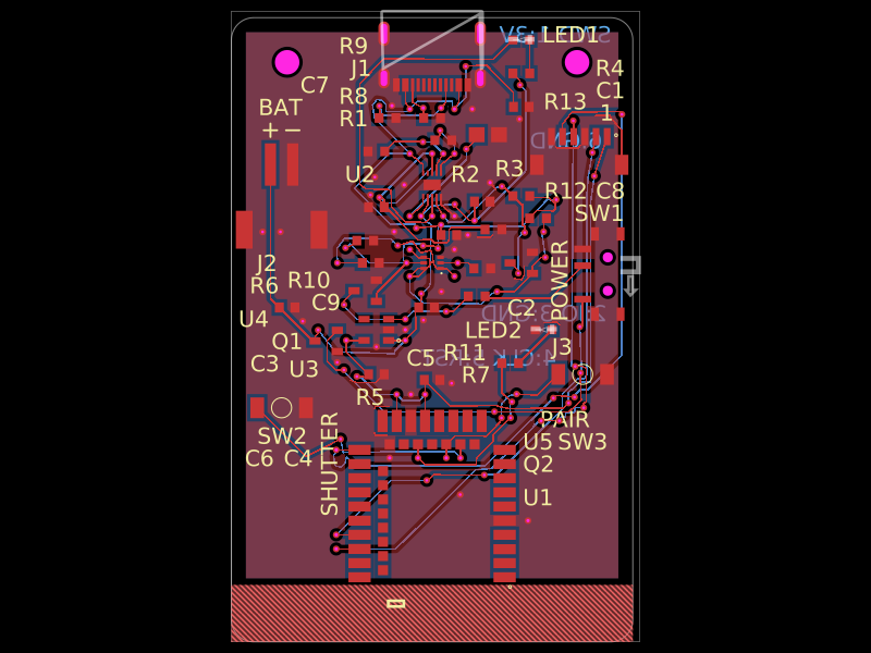 More from this authorAnasSarkiz/magnetic-shutter-remote--01a0f81fA compact USB‑C rechargeable battery device with BQ25185 charging, 3.3‑V regulation and protection, E73 Bluetooth control, temperature monitoring, status/charge LEDs, shutter/pair/power switches, and a mechanically enclosed Li‑Po battery with docking/antenna provisions.
 Similar packagemohan-bee/esp32-c3This hardware design integrates an ESP32-C3 microcontroller, a USB-C connector, a power management IC (AP2112-3.3V regulator), a USB-to-Serial converter (CH340C), several resistors, capacitors, and user-accessible headers to facilitate USB communication, power regulation, and general I/O interfacing.
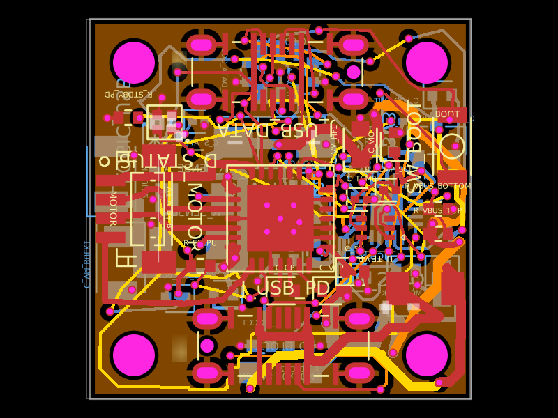 Discover something newShiboSoftwareDev/nema8-20mm-dual-usbc-stepper-controllerA compact 20 mm four-layer USB‑C stepper-controller PCB combining CH32X035 MCU control, TMC2209 motor driving, USB‑C PD/data interfaces, protection/power regulation, temperature/LED status hardware, and NEMA8 motor connectivity.