AnasSarkiz/muse-voice-remote
Muse Voice Remote — bare ESP32-S3R8, 155 TOP JLCPCB parts with real supplier CAD, native 3D assembly and GLB exports. Revised 17 mm case allocation; 0.30 mm via drill /0.45 mm pad. Checked prototype PCB; mechanical, RF and MUSE qualification pending.
- Version
- 1.3.2
- License
- unset
- Stars
- 0
vendor/espressif-bare-s3/pcb-layout-design.rst
.. _pcb-layout-design:

PCB Layout Design
========================
:link_to_translation:`zh_CN:[中文]`

This chapter introduces the key points of how to design an {IDF_TARGET_NAME} PCB layout using an {IDF_TARGET_NAME} module (see Figure :ref:`fig-pcb-layout-example`) as an example.

.. figure:: ../_static/{IDF_TARGET_PATH_NAME}/{IDF_TARGET_PATH_NAME}-pcb-layout-example.png
   :name: fig-pcb-layout-example
   :align: center
   :width: 50%
   :alt: {IDF_TARGET_NAME} Reference PCB Layout

   {IDF_TARGET_NAME} Reference PCB Layout

General Principles of PCB Layout for the Chip
----------------------------------------------

It is recommended to use a four-layer PCB design:

.. only:: not esp32s31

    - Layer 1 (TOP): Signal traces and components.
    - Layer 2 (GND): No signal traces here to ensure a complete GND plane.
    - Layer 3 (POWER): GND plane should be applied to better isolate the RF and crystal. Route power traces and a few signal traces on this layer, provided that there is a complete GND plane under the RF and crystal.
    - Layer 4 (BOTTOM): Route a few signal traces here. It is not recommended to place any components on this layer.

.. only:: esp32s31

    - Layer 1 (TOP): Apply ground copper. Mainly used for signal traces and components.
    - Layer 2 (GND): Apply ground copper. No signal traces here to ensure a complete GND plane.
    - Layer 3 (POWER): Apply ground copper. Route power traces on this layer. Signal traces are allowed.
    - Layer 4 (BOTTOM): Apply ground copper. Signal traces are allowed.


.. only:: not esp32c5 and not esp32s31

    A two-layer PCB design can also be used:

    - Layer 1 (TOP): Signal traces and components.
    - Layer 2 (BOTTOM): Do not place any components on this layer and keep traces to a minimum. Please make sure there is a complete GND plane for the chip, RF, and crystal.


.. only:: esp32s31

    A two-layer PCB design can also be used:

    - Layer 1 (TOP): Apply ground copper. Mainly used for components and routing.
    - Layer 2 (BOTTOM): Apply ground copper. Do not place any components on this layer and keep traces to a minimum. Please make sure there is a complete GND plane for the chip, RF, and crystal.


.. _pcb-layout-design-power-supply:

Power Supply
-----------------

{IDF_TARGET_POWER_TRACE_WIDTH:default="25", esp32c3="20", esp32c2="20", esp32h2="20", esp32c5="35", esp32s31="30"}

{IDF_TARGET_ANALOG_POWER_TRACE:default="VDD3P3", esp32c6="VDDA3P3", esp32c2="VDDA3P3", esp32h2="VDD3P3 at pin1 and pin2", esp32s2="VDD3P3 at pin3 and pin4", esp32c5="VDDA6, VDDA7, VDDA1, and VDDA2 at pin1, pin3, pin40, and pin41", esp32s3="VDD3P3 at pin2 and pin3", esp32s31="VDDA3 and VDDA4"}

{IDF_TARGET_ANALOG_POWER_TRACE_WIDTH:default="20", esp32c3="15", esp32c2="15", esp32h2="15"}

{IDF_TARGET_ANALOG_FILTER_CIRCUIT:default="CLC", esp32c3="LC", esp32c2="LC"}

{IDF_TARGET_RF_POWER_TRACE:default="pin2 and pin3", esp32c5="pin1, pin3, pin40, and pin41"}

.. only:: not esp32h2

    .. include:: shared/pcb-power-layout-four-layer.inc

.. only:: esp32h2

    .. include:: {IDF_TARGET_PATH_NAME}/{IDF_TARGET_PATH_NAME}-pcb-power-layout-four-layer.inc

.. only:: esp32 or esp32c3 or esp32s2 or esp32s3 or esp32c6 or esp32c61

    .. include:: shared/pcb-power-layout-two-layer.inc

.. _crystal-layout:

Crystal
----------

{IDF_TARGET_CRYSTAL_GAP:default="to be defined", esp32="2.7", esp32s2="2.0", esp32s3="2.0", esp32c3="2.0", esp32c6="2.4", esp32h2="1.8", esp32c2="2.0", esp32s2="2.0", esp32c5="2.4", esp32c61="2.4", esp32s31="1.7"}

.. only:: esp32

    Figure :ref:`fig-crystal-ref-design` shows a reference layout for crystal on {IDF_TARGET_NAME}.

    .. figure:: ../_static/{IDF_TARGET_PATH_NAME}/{IDF_TARGET_PATH_NAME}-crystal-ref-design.png
        :name: fig-crystal-ref-design
        :align: center
        :width: 70%
        :alt: {IDF_TARGET_NAME} Crystal Layout

        {IDF_TARGET_NAME} Crystal Layout

.. only:: not esp32c2 and not esp32s2 and not esp32c3 and not esp32

    Figure :ref:`fig-crystal-not-to-gnd` shows a reference PCB layout where the crystal is connected to the ground through vias and a keep-out area is maintained around the crystal on the top layer for ground isolation.

    .. figure:: ../_static/{IDF_TARGET_PATH_NAME}/{IDF_TARGET_PATH_NAME}-pcb-crystal-not-to-gnd.png
        :name: fig-crystal-not-to-gnd
        :align: center
        :width: 70%
        :alt: {IDF_TARGET_NAME} Crystal Layout (with Keep-out Area on Top Layer)

        {IDF_TARGET_NAME} Crystal Layout (with Keep-out Area on Top Layer)

.. only:: esp32s3 or esp32h2 or esp32c2 or esp32s2 or esp32c3

    Figure :ref:`fig-crystal-to-gnd` shows the layout for the crystal that is connected to the ground through vias but there is no keep-out area on the top layer for ground isolation.

    .. figure:: ../_static/{IDF_TARGET_PATH_NAME}/{IDF_TARGET_PATH_NAME}-pcb-crystal-to-gnd.png
        :name: fig-crystal-to-gnd
        :align: center
        :width: 60%
        :alt: {IDF_TARGET_NAME} Crystal Layout (without Keep-out Area on Top Layer)

        {IDF_TARGET_NAME} Crystal Layout (without Keep-out Area on Top Layer)

.. only:: esp32s3 or esp32h2 or esp32c5 or esp32c61 or esp32c6 or esp32s31

    If there is sufficient ground on the top layer, it is recommended to maintain a keep-out area around the crystal for ground isolation. This helps to reduce the value of parasitic capacitance and suppress temperature conduction, which can otherwise affect the frequency offset. If there is no sufficient ground, do not maintain any keep-out area.

The layout of the crystal should follow the guidelines below:

- Ensure a complete GND plane for the RF, crystal, and chip.
- The crystal should be placed far from the clock pin to avoid interference on the chip. The gap should be at least {IDF_TARGET_CRYSTAL_GAP} mm. It is good practice to add high-density ground vias stitching around the clock trace for better isolation.
- There should be no vias for the clock input and output traces.
- Components in series to the crystal trace should be placed close to the chip side.
- The external matching capacitors should be placed on the two sides of the crystal, preferably at the end of the clock trace, but not connected directly to the series components. This is to make sure the ground pad of the capacitor is close to that of the crystal.
- Do not route high-frequency digital signal traces under the crystal. It is best not to route any signal trace under the crystal. The vias on the power traces on both sides of the crystal clock trace should be placed as far away from the clock trace as possible, and the two sides of the clock trace should be surrounded by ground copper.
- As the crystal is a sensitive component, do not place any magnetic components nearby that may cause interference, for example large inductance component, and ensure that there is a clean large-area ground plane around the crystal.

.. _rf-layout:

RF
-----

{IDF_TARGET_STUB_LENGTH:default="15", esp32c5="10"}
{IDF_TARGET_RF_MATCHING_CIRCUIT:default="CLC", esp32c61="CLCCL", esp32c5="5G interface CLC", esp32c6="CLCCL", esp32s31="CLCCL"}

.. only:: esp32

    RF Layout on Four-layer PCB
    ^^^^^^^^^^^^^^^^^^^^^^^^^^^^

The RF trace is routed as shown highlighted in pink in Figure :ref:`fig-rf-layout`.

.. figure:: ../_static/{IDF_TARGET_PATH_NAME}/{IDF_TARGET_PATH_NAME}-pcb-rf-layout.png
    :name: fig-rf-layout
    :align: center
    :width: 50%
    :alt: {IDF_TARGET_NAME} RF Layout in a Four-layer PCB Design

    {IDF_TARGET_NAME} RF Layout in a Four-layer PCB Design

The RF layout should meet the following guidelines:

.. list::

    :not esp32s31: - The RF trace should have a 50 Ω characteristic impedance. The reference plane is the layer next to the chip. For designing the RF trace at 50 Ω impedance, you could refer to the PCB stack-up design shown below.
    :esp32s31: - The RF trace should have a 50 Ω characteristic impedance. The reference plane is the third layer. For designing the RF trace at 50 Ω impedance, you could refer to the PCB stack-up design shown below.

.. only:: not esp32s31

    .. figure:: ../_static/shared-stackup-design__en.png
        :name: fig-stackup-design
        :align: center
        :width: 90%
        :alt: {IDF_TARGET_NAME} PCB Stack up Design

        {IDF_TARGET_NAME} PCB Stack-up Design

.. only:: esp32s31

    .. figure:: ../_static/{IDF_TARGET_PATH_NAME}/{IDF_TARGET_PATH_NAME}-pcb-stackup-design__en.png
        :name: fig-stackup-design
        :align: center
        :width: 90%
        :alt: {IDF_TARGET_NAME} PCB Stack-up Design

        {IDF_TARGET_NAME} PCB Stack-up Design

.. only:: esp32s31

    .. attention::

        The third layer is used as the reference plane for this module because, with the current stack-up structure, the RF trace width differs too much from the component pad size. To avoid abrupt transitions from the trace to component pads, the area under the RF trace on the second layer is cleared, and the third layer is used as the reference ground plane to obtain RF traces of suitable width.

        If the stack-up used does not have this issue, it is recommended to use the layer adjacent to the chip as the reference ground plane.

.. list::

    :esp32c5: - At least one CLC matching circuit is required for chip tuning. Please use 0201 components and place them close to the pin in a zigzag. In other words, the two capacitors should not be oriented in the same direction to minimize interference.
    :not esp32c5: - A {IDF_TARGET_RF_MATCHING_CIRCUIT} matching circuit is required for chip tuning. Please use 0201 components and place them close to the pin in a zigzag. In other words, the two capacitors should not be oriented in the same direction to minimize interference.
    :esp32s2: - Add a stub on the grounding capacitor near the chip side in the CLC matching circuit to suppress the second harmonics. It is preferable to keep the stub length {IDF_TARGET_STUB_LENGTH} mil, and determine the stub width according to the PCB stack-up so that the characteristic impedance of the stub is 100 Ω ± 10%. In addition, connect the stub ground vias to the third layer, and maintain a keep-out area on the first and second layers. Note that a stub is not required when the CLC matching circuit components use package types of 0402 or larger.
    :not esp32s2: - Add a stub on the ground pad of the grounding capacitor near the chip side in the matching circuit to suppress the second harmonics. It is preferable to keep the stub length {IDF_TARGET_STUB_LENGTH} mil, and determine the stub width according to the PCB stack-up so that the characteristic impedance of the stub is 100 Ω ± 10%. The reference plane is the third layer, so the area under the trace on the second layer should be cleared. The trace highlighted in Figure :ref:`fig-stub-layout` is the stub. Note that a stub is not required for package types of 0402 and above.
    :esp32s3 or esp32c5 or esp32 or esp32c61 or esp32c6 or esp32s31: - It is recommended to keep all layers clear under the IPEX antenna connector. See Figure :ref:`fig-pcb-ipex-layout`.
    - For PCB antennas, make sure to validate them through both simulation and real-world testing on a development board. It is recommended to include an additional CLC matching circuit for antenna tuning. Place this circuit as close to the antenna as possible.

.. only:: not esp32s2

    .. figure:: ../_static/{IDF_TARGET_PATH_NAME}/{IDF_TARGET_PATH_NAME}-pcb-stub-layout.png
        :name: fig-stub-layout
        :align: center
        :width: 50%
        :alt: {IDF_TARGET_NAME} Stub in a Four-layer PCB Design

        {IDF_TARGET_NAME} Stub in a Four-layer PCB Design

.. only:: esp32s3 or esp32c5 or esp32 or esp32c61 or esp32c6 or esp32s31

    .. figure:: ../_static/{IDF_TARGET_PATH_NAME}/{IDF_TARGET_PATH_NAME}-pcb-ipex-layout.png
        :name: fig-pcb-ipex-layout
        :align: center
        :width: 50%
        :alt: {IDF_TARGET_NAME} IPEX Antenna Connector Layout

        {IDF_TARGET_NAME} IPEX Antenna Connector Layout

- The RF trace should have a consistent width and not branch out. It should be as short as possible with dense ground vias around for interference shielding.
- The RF trace should be routed on the outer layer without vias, i.e., should not cross layers. The RF trace should be routed at a 135° angle, or with circular arcs if trace bends are required.
- The ground plane on the adjacent layer needs to be complete. Do not route any traces under the RF trace whenever possible.
- There should be no high-frequency signal traces routed close to the RF trace. The RF antenna should be placed away from high-frequency components, such as crystals, DDR SDRAM, high-frequency clocks, etc. In addition, the USB port, USB-to-serial chip, UART signal lines (including traces, vias, test points, header pins, etc.) must be as far away from the antenna as possible. The UART signal line should be surrounded by ground copper and ground vias.

.. only:: esp32

    RF Layout on Two-layer PCB
    ^^^^^^^^^^^^^^^^^^^^^^^^^^^^

    .. include:: {IDF_TARGET_PATH_NAME}/{IDF_TARGET_PATH_NAME}-rf-layout-two-layer-pcb-design.inc

.. only:: esp32 or esp32s3 or esp32c3 or esp32c6 or esp32s2 or esp32c5 or esp32c61 or esp32s31

    {IDF_TARGET_FLASH_PSRAM:default="Flash", esp32="Flash and PSRAM", esp32s3="Flash and PSRAM", esp32s2="Flash and PSRAM", esp32c5="Flash and PSRAM", esp32c61="Flash and PSRAM", esp32s31="Flash and PSRAM"}

    {IDF_TARGET_FLASH_PSRAM_CASE:default="flash", esp32="flash and PSRAM", esp32s3="flash and PSRAM", esp32s2="flash and PSRAM", esp32s31="flash and PSRAM"}

    {IDF_TARGET_VDD_POWER:default="VDD_SPI", esp32="VDD_SDIO"}

    {IDF_TARGET_FLASH_PSRAM}
    ---------------------------

    The layout for {IDF_TARGET_FLASH_PSRAM_CASE} should follow the guidelines below:

    .. list::

        - Place the zero-ohm resistors in series on the SPI lines close to {IDF_TARGET_NAME}.
        - Route the SPI traces on the inner layer (e.g., the third layer) whenever possible, and add ground copper and ground vias around the clock and data traces of SPI separately.
        :esp32s3: - Octal SPI traces should have matching lengths.
        :esp32c5 or esp32 or esp32s3 or esp32c3 or esp32c6 or esp32s2 or esp32c61 or esp32s31: - If the flash and PSRAM are located far from {IDF_TARGET_NAME}, it is recommended to place appropriate decoupling capacitors both at {IDF_TARGET_VDD_POWER} and near the flash and PSRAM power supply.

    .. only:: not esp32 and not esp32s2

        Figure :ref:`fig-flash-layout` shows the quad SPI flash layout.

        .. figure:: ../_static/{IDF_TARGET_PATH_NAME}/{IDF_TARGET_PATH_NAME}-pcb-flash-layout.png
            :name: fig-flash-layout
            :align: center
            :width: 70%
            :alt: {IDF_TARGET_NAME} Quad SPI Flash Layout

            {IDF_TARGET_NAME} Quad SPI Flash Layout

    .. only:: esp32

        Figure :ref:`fig-flash-layout` shows an example of flash (U3) and PSRAM (U4) layout.

        .. figure:: ../_static/{IDF_TARGET_PATH_NAME}/{IDF_TARGET_PATH_NAME}-pcb-flash-layout.png
            :name: fig-flash-layout
            :align: center
            :width: 70%
            :alt: {IDF_TARGET_NAME} Flash and PSRAM Layout

            {IDF_TARGET_NAME} Flash and PSRAM Layout

    .. only:: esp32s2

        Figure :ref:`fig-flash-layout` shows an example of flash and PSRAM layout.

        .. figure:: ../_static/{IDF_TARGET_PATH_NAME}/{IDF_TARGET_PATH_NAME}-pcb-flash-layout.png
            :name: fig-flash-layout
            :align: center
            :width: 70%
            :alt: {IDF_TARGET_NAME} Flash and PSRAM Layout

            {IDF_TARGET_NAME} Flash and PSRAM Layout

    .. only:: esp32s3

        Figure :ref:`fig-octal-flash-layout` shows the octal SPI flash layout.

        .. figure:: ../_static/{IDF_TARGET_PATH_NAME}/{IDF_TARGET_PATH_NAME}-pcb-octal-flash-layout.png
            :name: fig-octal-flash-layout
            :align: center
            :width: 70%
            :alt: {IDF_TARGET_NAME} Octal SPI Flash Layout

            {IDF_TARGET_NAME} Octal SPI Flash Layout

.. only:: esp32

    External RC
    ----------------------

    External resistors and capacitors should be placed close to the chip pins, and there should be no vias around the traces. Please ensure that 10 nF capacitors are placed close to the pins.

UART
---------

.. only:: not esp32s2

    Figure :ref:`fig-uart-layout` shows the UART layout.

    .. figure:: ../_static/{IDF_TARGET_PATH_NAME}/{IDF_TARGET_PATH_NAME}-pcb-uart-layout.png
        :name: fig-uart-layout
        :align: center
        :width: 60%
        :alt: {IDF_TARGET_NAME} UART Layout

        {IDF_TARGET_NAME} UART Layout

The UART layout should meet the following guidelines:

- The series resistor on the U0TXD trace needs to be placed close to the chip side and away from the crystal.
- The U0TXD and U0RXD traces on the top layer should be as short as possible.
- The UART trace should be surrounded by ground copper and ground vias stitching.

.. _pcb-layout-design-on-a-base-board:

General Principles of PCB Layout for Modules (Positioning a Module on a Base Board)
-----------------------------------------------------------------------------------

{IDF_TARGET_ANTENNA_POINT:default="feed point", esp32c5="GND point"}

{IDF_TARGET_ANTENNA_POINT_POSITION:default="right", esp32h2="left", esp32c2="left", esp32s31="left"}

If module-on-board design is adopted, attention should be paid while positioning the module on the base board. The interference of the baseboard on the module's antenna performance should be minimized.

It is suggested to place the module's on-board PCB antenna outside the base board, and the {IDF_TARGET_ANTENNA_POINT} of the antenna close to the edge of the base board. In the following example figures, positions with mark ✓ are strongly recommended, while positions without a mark are not recommended.

.. only:: not esp32c2 and not esp32s31

    .. figure:: ../_static/{IDF_TARGET_PATH_NAME}/{IDF_TARGET_PATH_NAME}-module-place-on-base-board-right.png
        :name: fig-module-place-on-base-board-right
        :align: center
        :width: 85%
        :alt: Placement of {IDF_TARGET_NAME} Modules on Base Board (antenna {IDF_TARGET_ANTENNA_POINT} on the right)

        Placement of {IDF_TARGET_NAME} Modules on Base Board (antenna {IDF_TARGET_ANTENNA_POINT} on the right)

.. only:: not esp32s2 and not esp32c5

    .. figure:: ../_static/{IDF_TARGET_PATH_NAME}/{IDF_TARGET_PATH_NAME}-module-place-on-base-board-left.png
        :name: fig-module-place-on-base-board-left
        :align: center
        :width: 85%
        :alt: Placement of {IDF_TARGET_NAME} Modules on Base Board (antenna {IDF_TARGET_ANTENNA_POINT} on the left)

        Placement of {IDF_TARGET_NAME} Modules on Base Board (antenna {IDF_TARGET_ANTENNA_POINT} on the left)

If the antenna cannot extend beyond the board edge, the {IDF_TARGET_ANTENNA_POINT} should still be placed as close to the board edge as possible. Then cut off the base board on both sides of the antenna and below it to minimize the impact of the base board material on the PCB antenna and provide a sufficiently large clearance area for the PCB antenna. Note that the module should not be placed in the center of the board with clearance created by hollowing out on all four sides. Figure :ref:`fig-module-clearance` shows the suggested clearance area. Please note that sufficient ground copper and dense ground vias should be placed on the base board near the antenna.

.. figure:: ../_static/{IDF_TARGET_PATH_NAME}/{IDF_TARGET_PATH_NAME}-module-clearance.png
    :name: fig-module-clearance
    :align: center
    :width: 75%
    :alt: Keepout Zone for {IDF_TARGET_NAME} Module's Antenna (Antenna {IDF_TARGET_ANTENNA_POINT} on the {IDF_TARGET_ANTENNA_POINT_POSITION})

    Keepout Zone for {IDF_TARGET_NAME} Module's Antenna (Antenna {IDF_TARGET_ANTENNA_POINT} on the {IDF_TARGET_ANTENNA_POINT_POSITION})

After the base board is placed in the end product, please consider the impact of the housing on the antenna during end-product design. Ensure that the PCB antenna on the base board also has a sufficiently large clearance area inside the housing. A clearance of at least 15 mm is recommended in all directions.

Please note that the final end product should be tested for throughput and communication range to ensure RF performance.


.. only:: esp32s31

    .. _adc-layout:

    ADC
    --------

    The ADC layout should follow the guidelines below:

    - For high-precision ADC, the P and N traces should be routed close together with a spacing of 1~1.5 times the trace width between them. Ensure ground isolation from other traces.


.. only:: esp32s3 or esp32c3 or esp32c6 or esp32h2 or esp32s2 or esp32c5 or esp32c61 or esp32s31

    .. _usb-layout:

    USB
    -------

    The USB layout should meet the following guidelines:

    - Reserve space for resistors and capacitors on the USB traces close to the chip side.
    - Use differential pairs and route them in parallel at equal lengths. Maintain a differential pair impedance of 90 Ω with a tolerance of ±10%.
    - USB differential traces should minimize via transitions as much as possible to ensure better impedance control and avoid signal reflections. If vias are necessary, add a pair of ground return vias at each transition point.
    - Ensure there is a continuous reference layer (a ground layer is recommended) beneath the USB traces.
    - Surround the USB traces with ground copper.

.. only:: esp32 or esp32s3 or esp32c6 or esp32c5 or esp32c61 or esp32s31

    .. _sdio-layout:

    SDIO
    --------

    The SDIO layout should follow the guidelines below:

    .. list::

        - Minimize parasitic capacitance of SDIO traces as they involve high-speed signals.
        - The trace lengths for SDIO_CMD and SDIO_DATA0 ~ SDIO_DATA3 should be within ± 50 mil of the SDIO_CLK trace length. Use serpentine routing if necessary.
        - For SDIO routing, maintain a 50 Ω single-ended impedance with a tolerance of ±10%.
        - Keep the total trace length from SDIO GPIOs to the master SDIO interface as short as possible, ideally within 2000 mil.
        - Ensure that SDIO traces do not cross layers. Besides, a reference plane (preferably a ground plane) must be placed beneath the traces, and continuity of the reference plane must be ensured.
        - It is recommended to surround the SDIO_CLK trace with ground copper.
        :esp32c61: - For multi-layer PCB designs, it is recommended to route the SDIO traces to the inner layers immediately after exiting the chip through vias, in order to reduce interference on high-speed signal lines. Additionally, place a pair of ground vias near the layer transition to ensure proper return path.

    .. only:: esp32c5

        .. note::

            This peripheral is supported by the chip revision v1.0, but not by v0.1.


.. only:: esp32 or esp32s3 or esp32s2 or esp32s31

    Touch Sensor
    --------------

    .. include:: {IDF_TARGET_PATH_NAME}/{IDF_TARGET_PATH_NAME}-touch-sensor-design.inc

    Electrode Pattern
    ^^^^^^^^^^^^^^^^^^^^^

    .. include:: {IDF_TARGET_PATH_NAME}/{IDF_TARGET_PATH_NAME}-touch-sensor-electrode-pattern.inc

    PCB Layout
    ^^^^^^^^^^^^^

    .. include:: {IDF_TARGET_PATH_NAME}/{IDF_TARGET_PATH_NAME}-touch-sensor-pcb-layout.inc

    .. only:: esp32s3 or esp32s31

        Waterproof and Proximity Sensing Design
        ^^^^^^^^^^^^^^^^^^^^^^^^^^^^^^^^^^^^^^^^^

        .. include:: {IDF_TARGET_PATH_NAME}/{IDF_TARGET_PATH_NAME}-touch-sensor-waterproof-design.inc

    .. note::

        For more details on the hardware design of the touch sensor, please refer to `Touch Sensor Application Note <https://github.com/espressif/esp-iot-solution/blob/release/v1.0/documents/touch_pad_solution/touch_sensor_design_en.md>`_.


.. only:: esp32s31

    .. _emac-layout:

    EMAC
    --------

    The EMAC layout should follow the guidelines below:

    - EMAC traces should maintain a 50 Ω single-ended impedance with a tolerance of ±10%.
    - EMAC traces should follow the basic 3W rule for high-speed digital circuit routing.
    - For the MII/RGMII interface, TX data trace lengths should be within ± 50 mil of the TX_CLK trace length, and RX data trace lengths should be within ± 50 mil of the RX_CLK trace length. Use serpentine routing if necessary.
    - A reference layer must be placed beneath EMAC traces, and continuity of the reference layer must be ensured.
    - For multi-layer PCB designs, it is recommended to route EMAC traces to the inner layers immediately after exiting the chip through vias, in order to reduce interference on high-speed signal lines. Additionally, place a pair of ground vias near the layer transition to ensure proper return path.
    - EMAC traces should be isolated from other traces with ground copper.

Typical Layout Problems and Solutions
-------------------------------------------

.. include:: shared/faq.inc
Related Packages
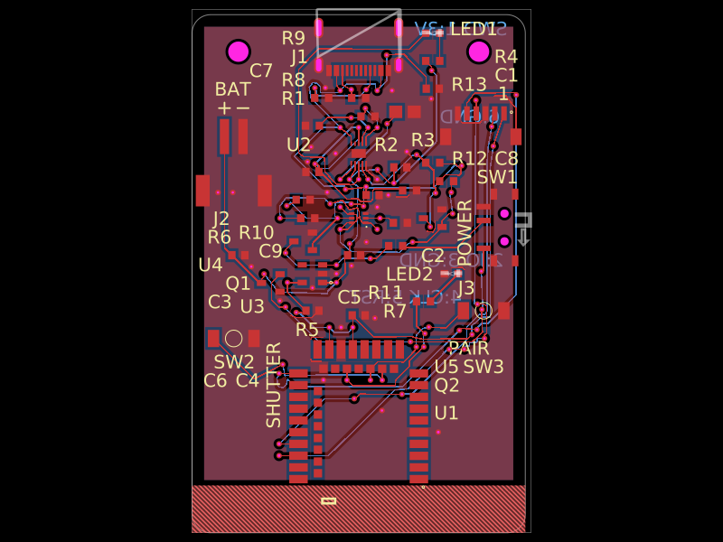 More from this authorAnasSarkiz/magnetic-shutter-remote--01a0f81fA compact USB‑C rechargeable battery device with BQ25185 charging, 3.3‑V regulation and protection, E73 Bluetooth control, temperature monitoring, status/charge LEDs, shutter/pair/power switches, and a mechanically enclosed Li‑Po battery with docking/antenna provisions.
 Similar packagemohan-bee/esp32-c3This hardware design integrates an ESP32-C3 microcontroller, a USB-C connector, a power management IC (AP2112-3.3V regulator), a USB-to-Serial converter (CH340C), several resistors, capacitors, and user-accessible headers to facilitate USB communication, power regulation, and general I/O interfacing.
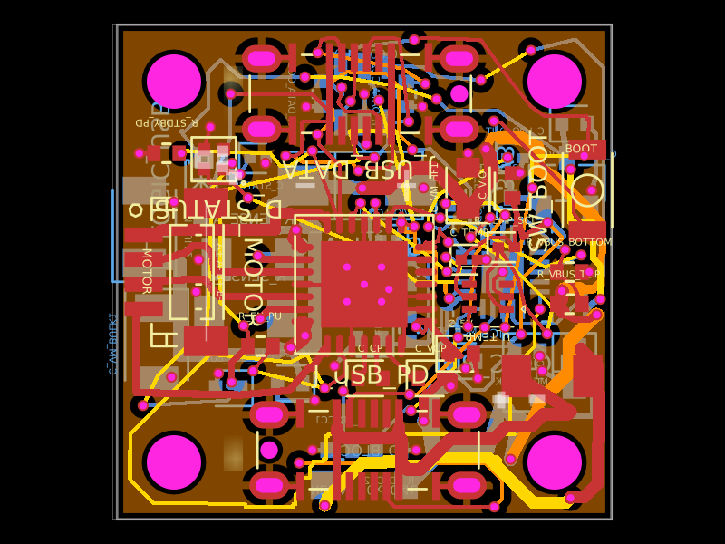 Discover something newShiboSoftwareDev/nema8-20mm-dual-usbc-stepper-controllerA compact 20 mm four-layer USB‑C stepper-controller PCB combining CH32X035 MCU control, TMC2209 motor driving, USB‑C PD/data interfaces, protection/power regulation, temperature/LED status hardware, and NEMA8 motor connectivity.