AnasSarkiz/muse-voice-remote
Muse Voice Remote — bare ESP32-S3R8, 155 TOP JLCPCB parts with real supplier CAD, native 3D assembly and GLB exports. Revised 17 mm case allocation; 0.30 mm via drill /0.45 mm pad. Checked prototype PCB; mechanical, RF and MUSE qualification pending.
- Version
- 1.3.2
- License
- unset
- Stars
- 0
scripts/routed-overlay.ts
import { readFileSync } from "node:fs"
import { createHash } from "node:crypto"
import type { AnyCircuitElement } from "circuit-json"
import copper from "../design/routed-copper.json"

export function addVerifiedCopper(json: AnyCircuitElement[]) {
  const inputHash=createHash("sha256").update(readFileSync("docs/routing-input.json")).digest("hex")
  if (inputHash!==copper.input_sha256) throw new Error("Wiring or placement changed: native routes need to be updated and checked.")
  const cadHash=createHash("sha256").update(readFileSync("hardware/MuseVoiceRemote.kicad_pcb")).digest("hex")
  if (cadHash!==copper.cad_sha256) throw new Error("Native CAD changed without an updated DRC/route snapshot.")
  const nets=json.filter(e=>e.type==="source_net")
  const traces=json.filter(e=>e.type==="source_trace")
  const board=json.find(e=>e.type==="pcb_board")!
  const sourceFor=(name:string)=>{
    const net=nets.find(n=>n.name===name)
    const trace=traces.find(t=>net && t.connected_source_net_ids?.includes(net.source_net_id))
    if (!trace) throw new Error(`No tscircuit source net for native copper ${name}`)
    return trace.source_trace_id
  }
  for (const [i,t] of copper.tracks.entries()) json.push({ type:"pcb_trace",pcb_trace_id:`native_trace_${i}`,
    source_trace_id:sourceFor(t.net),subcircuit_id:board.subcircuit_id,
    route:[t.start,t.end].map(([x,y])=>({ route_type:"wire",x,y,width:t.width,layer:t.layer })) } as AnyCircuitElement)
  for (const [i,v] of copper.vias.entries()) json.push({ type:"pcb_via",pcb_via_id:`native_via_${i}`,
    source_trace_id:sourceFor(v.net),subcircuit_id:board.subcircuit_id,
    x:v.at[0],y:v.at[1],outer_diameter:v.outerDiameter,hole_diameter:v.holeDiameter,
    from_layer:"top",to_layer:"bottom",layers:["top","inner1","inner2","bottom"] } as AnyCircuitElement)
  // Retain the actual filled native geometry, including every clearance hole.
  // A rectangular approximation would short foreign pads and tracks.
  const pours=(copper as typeof copper & {pours?:{
    net:string;layer:string;brep_shape:{outer_ring:{vertices:{x:number;y:number}[]};inner_rings:{vertices:{x:number;y:number}[]}[]}
  }[]}).pours ?? []
  for(const [i,p] of pours.entries()) {
    const net=nets.find(n=>n.name===p.net)
    if(!net)throw new Error(`No source net for native plane ${p.net}`)
    json.push({type:"pcb_copper_pour",pcb_copper_pour_id:`native_pour_${i}`,
      source_net_id:net.source_net_id,subcircuit_id:board.subcircuit_id,
      layer:p.layer,covered_with_solder_mask:true,shape:"brep",brep_shape:p.brep_shape} as AnyCircuitElement)
  }
  return copper
}
Related Packages
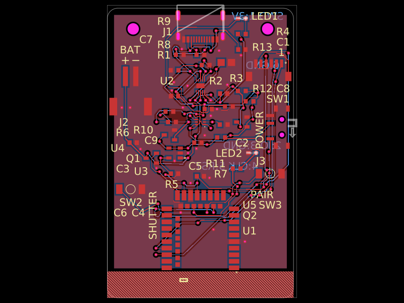 More from this authorAnasSarkiz/magnetic-shutter-remote--01a0f81fA compact USB‑C rechargeable battery device with BQ25185 charging, 3.3‑V regulation and protection, E73 Bluetooth control, temperature monitoring, status/charge LEDs, shutter/pair/power switches, and a mechanically enclosed Li‑Po battery with docking/antenna provisions.
 Similar packagemohan-bee/esp32-c3This hardware design integrates an ESP32-C3 microcontroller, a USB-C connector, a power management IC (AP2112-3.3V regulator), a USB-to-Serial converter (CH340C), several resistors, capacitors, and user-accessible headers to facilitate USB communication, power regulation, and general I/O interfacing.
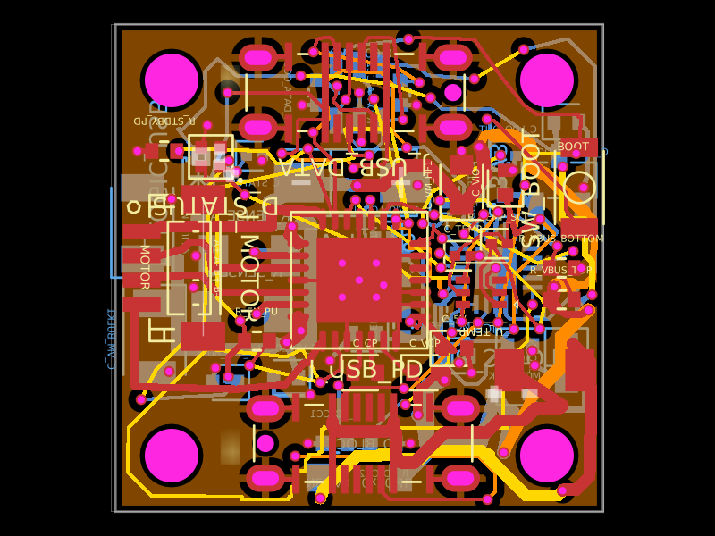 Discover something newShiboSoftwareDev/nema8-20mm-dual-usbc-stepper-controllerA compact 20 mm four-layer USB‑C stepper-controller PCB combining CH32X035 MCU control, TMC2209 motor driving, USB‑C PD/data interfaces, protection/power regulation, temperature/LED status hardware, and NEMA8 motor connectivity.