AnasSarkiz/muse-voice-remote
Muse Voice Remote — bare ESP32-S3R8, 155 TOP JLCPCB parts with real supplier CAD, native 3D assembly and GLB exports. Revised 17 mm case allocation; 0.30 mm via drill /0.45 mm pad. Checked prototype PCB; mechanical, RF and MUSE qualification pending.
- Version
- 1.3.2
- License
- unset
- Stars
- 0
scripts/native-board.py
#!/usr/bin/env python3
"""Use original imported KiCad files for the independent routing/DRC handoff.

This avoids regenerating or simplifying custom pad shapes, USB slots, paste,
mask and thermal holes in interchange exporters. No new footprint is authored.
"""
import json
import pathlib
import statistics
import math
import pcbnew
from chip_native import seed_chip_copper

root = pathlib.Path(__file__).resolve().parents[1]
catalog = json.loads((root / "docs/component-catalog.json").read_text())
rendered = json.loads((root / "dist/circuit.json").read_text())
rendered_sources = {e["name"]: e["source_component_id"] for e in rendered if e["type"] == "source_component"}
anchor_offsets = {}
board = pcbnew.BOARD()
board.SetCopperLayerCount(4)
board.GetDesignSettings().SetBoardThickness(pcbnew.FromMM(1))
settings = board.GetDesignSettings()
settings.m_MinThroughDrill = pcbnew.FromMM(0.3)  # Routing vias; imported MCU thermal holes also meet 0.30 mm.
settings.m_HoleClearance = pcbnew.FromMM(0.15)   # Connector's qualified geometry requires this capability.
settings.m_CopperEdgeClearance = pcbnew.FromMM(0.5)
settings.m_MinClearance = pcbnew.FromMM(0.15)
names = sorted({net for p in catalog if p.get("library") for net in p["padNets"].values()})
nets = {}
for code, name in enumerate(names,1):
    net = pcbnew.NETINFO_ITEM(board,name,code)
    board.Add(net)
    nets[name] = net

for part in catalog:
    if not part.get("library"):
        continue
    name = part["library"].split("/")[1]
    directory = "vendor/jlcpcb/library" if part["library"].startswith("JLCPCB/") else "vendor/library"
    footprint = pcbnew.FootprintLoad(str(root / directory),name)
    if footprint is None:
        raise RuntimeError(f"Could not import {part['library']}")
    footprint.SetReference(part["reference"])
    footprint.SetValue(part["mpn"])
    # All currently selected populated parts have SMT electrical terminals.
    # Some supplier entries omit SMT metadata, so the converter labels their
    # footprint through-hole despite containing only SMD solder lands. Keep
    # the original pads and holes, but classify the assembly component as SMD.
    footprint.SetAttributes(pcbnew.FP_SMD)
    # KiCad uses +Y downward; tscircuit uses +Y upward.
    footprint.SetPosition(pcbnew.VECTOR2I(pcbnew.FromMM(part["x"]),pcbnew.FromMM(-part["y"])))
    footprint.SetOrientationDegrees(part["rotation"])
    # The assembly/BOM retains every reference. Hide long library fields on
    # physical silk so reference text cannot cover adjacent fine-pitch pads.
    footprint.Reference().SetVisible(False)
    footprint.Value().SetVisible(False)
    imported_ports = []
    if part["library"].startswith("JLCPCB/"):
        imported_ports = [p for p in json.loads((root / f"vendor/jlcpcb/{name}.circuit.json").read_text()) if p["type"] == "source_port"]
        # The supplier's native origin and tscircuit's recentered origin can
        # differ. Align board placement through actual imported pad centers;
        # do not move or redraw any pad inside its library footprint.
        placed = next(e for e in rendered if e["type"] == "pcb_component" and e["source_component_id"] == rendered_sources[part["reference"]])
        targets = [e for e in rendered if e.get("pcb_component_id") == placed["pcb_component_id"] and e["type"] in ["pcb_smtpad", "pcb_plated_hole"] and "x" in e]
        deltas = []
        for pad in footprint.Pads():
            key = pad.GetNumber()
            if not key: continue
            if not key.isdigit():
                port = next((p for p in imported_ports if key in p.get("port_hints", [])), None)
                if not port: continue
                key = str(port["pin_number"])
            matches = [e for e in targets if f"pin{key}" in e.get("port_hints", [])]
            if len(matches) != 1: continue
            target = matches[0]
            at = pad.GetPosition()
            deltas.append((target["x"]-pcbnew.ToMM(at.x), -target["y"]-pcbnew.ToMM(at.y)))
        if not deltas: raise RuntimeError(f"No pad alignment for {part['reference']}")
        dx = statistics.median(p[0] for p in deltas)
        dy = statistics.median(p[1] for p in deltas)
        # easyeda2kicad exports positions rounded to 0.01 mm.
        if max(math.dist((dx,dy),p) for p in deltas) > 0.02:
            raise RuntimeError(f"Imported pad coordinate mismatch: {part['reference']}")
        footprint.Move(pcbnew.VECTOR2I(pcbnew.FromMM(dx), pcbnew.FromMM(dy)))
        anchor_offsets[part["reference"]] = {"dx":dx,"dy":dy}
    for pad in footprint.Pads():
        number = pad.GetNumber()
        key = number
        # The JLCPCB PH connector uses pad 0 for both mechanical tabs;
        # the tscircuit importer exposes that shared pad as logical pin4.
        if part["reference"] == "J_BAT" and number == "0": key = "4"
        if imported_ports and not number.isdigit():
            matched = next((p for p in imported_ports if number and number in p.get("port_hints", [])), None)
            if matched: key = str(matched["pin_number"])
        if key in part["padNets"]:
            pad.SetNet(nets[part["padNets"][key]])
    # Keep supplied library markings in the assembly/Fab layer. Their generic
    # silk outlines can cross the imported land pattern; copper/mask/paste are
    # untouched and native DRC warnings remain enabled.
    if part["library"].startswith("JLCPCB/"):
        for graphic in footprint.GraphicalItems():
            if graphic.GetLayer() == pcbnew.F_SilkS: graphic.SetLayer(pcbnew.F_Fab)
    board.Add(footprint)

for start, end in [((-33,-24),(33,-24)),((33,-24),(33,24)),((33,24),(-33,24)),((-33,24),(-33,-24))]:
    line = pcbnew.PCB_SHAPE()
    line.SetShape(pcbnew.SHAPE_T_SEGMENT)
    line.SetStart(pcbnew.VECTOR2I(pcbnew.FromMM(start[0]),pcbnew.FromMM(start[1])))
    line.SetEnd(pcbnew.VECTOR2I(pcbnew.FromMM(end[0]),pcbnew.FromMM(end[1])))
    line.SetLayer(pcbnew.Edge_Cuts)
    line.SetWidth(pcbnew.FromMM(0.05))
    board.Add(line)

# Copper keepout strips make the board-edge rule visible to SPECCTRA routers.
# Pads remain allowed (USB shell overhang); new tracks and vias must stay inside.
for xmin,ymin,xmax,ymax in [(-33,-24,-32.5,24),(32.5,-24,33,24),(-33,-24,33,-23.5),(-33,23.5,33,24)]:
    zone = pcbnew.ZONE(board)
    zone.SetIsRuleArea(True)
    layers = pcbnew.LSET()
    for layer in [pcbnew.F_Cu,pcbnew.In1_Cu,pcbnew.In2_Cu,pcbnew.B_Cu]: layers.AddLayer(layer)
    zone.SetLayerSet(layers)
    zone.SetDoNotAllowTracks(True)
    zone.SetDoNotAllowVias(True)
    zone.SetDoNotAllowPads(False)
    zone.SetDoNotAllowCopperPour(True)
    outline = zone.Outline()
    outline.NewOutline()
    for x,y in [(xmin,ymin),(xmax,ymin),(xmax,ymax),(xmin,ymax)]:
        outline.Append(pcbnew.FromMM(x),pcbnew.FromMM(y))
    board.Add(zone)

for x in [-31.5,31.5]:
    for y in [-22,22]:
        # Mechanical board hole, not an electronic/BOM component.
        footprint = pcbnew.FOOTPRINT(board)
        # SPECCTRA needs a nonempty image identifier, including board features.
        footprint.SetFPID(pcbnew.LIB_ID("", "PCB_MountingHole_1.8mm"))
        footprint.SetReference(f"H{len([p for p in board.GetFootprints() if p.GetReference().startswith('H')])+1}")
        footprint.SetValue("PCB mounting hole 1.8 mm")
        pad = pcbnew.PAD(footprint)
        pad.SetAttribute(pcbnew.PAD_ATTRIB_NPTH)
        pad.SetShape(pcbnew.PAD_SHAPE_CIRCLE)
        pad.SetSize(pcbnew.VECTOR2I(pcbnew.FromMM(1.8),pcbnew.FromMM(1.8)))
        pad.SetDrillSize(pcbnew.VECTOR2I(pcbnew.FromMM(1.8),pcbnew.FromMM(1.8)))
        pad.SetLayerSet(pcbnew.LSET.AllCuMask())
        footprint.Add(pad)
        footprint.SetPosition(pcbnew.VECTOR2I(pcbnew.FromMM(x),pcbnew.FromMM(y)))
        board.Add(footprint)

        # Reserve the assembly post/screw-head envelope on every copper layer.
        # This is a mechanical keepout, not a new electronic footprint.
        keepout=pcbnew.ZONE(board)
        keepout.SetIsRuleArea(True)
        copper=pcbnew.LSET()
        for layer in [pcbnew.F_Cu,pcbnew.In1_Cu,pcbnew.In2_Cu,pcbnew.B_Cu]:copper.AddLayer(layer)
        keepout.SetLayerSet(copper)
        keepout.SetDoNotAllowTracks(True);keepout.SetDoNotAllowVias(True)
        keepout.SetDoNotAllowPads(False);keepout.SetDoNotAllowCopperPour(True)
        polygon=keepout.Outline();polygon.NewOutline()
        for index in range(48):
            angle=2*math.pi*index/48
            polygon.Append(pcbnew.FromMM(x+1.8*math.cos(angle)),pcbnew.FromMM(y+1.8*math.sin(angle)))
        board.Add(keepout)

# Preserve explicit bottom-edge escape vias for the two microphone data pads.
# SPECCTRA routes from these accessible landings instead of attempting a
# fanout through each microphone's original custom ground-ring geometry.
for ref in [] if all(p["library"].startswith("JLCPCB/") for p in catalog) else ["MIC1","MIC2"]:
    footprint=next(f for f in board.GetFootprints() if f.GetReference()==ref)
    data_pad=next(p for p in footprint.Pads() if p.GetNumber()=="6")
    landing=pcbnew.VECTOR2I(data_pad.GetPosition().x,pcbnew.FromMM(-23.2))
    via=pcbnew.PCB_VIA(board)
    via.SetPosition(landing)
    for layer in [pcbnew.F_Cu,pcbnew.In1_Cu,pcbnew.In2_Cu,pcbnew.B_Cu]:
        via.SetWidth(layer,pcbnew.FromMM(0.6))
    via.SetDrill(pcbnew.FromMM(0.3))
    via.SetViaType(pcbnew.VIATYPE_THROUGH)
    via.SetLayerPair(pcbnew.F_Cu,pcbnew.B_Cu)
    via.SetNet(nets["MIC_SD"])
    board.Add(via)
    track=pcbnew.PCB_TRACK(board)
    track.SetStart(data_pad.GetPosition())
    track.SetEnd(landing)
    track.SetLayer(pcbnew.F_Cu)
    track.SetWidth(pcbnew.FromMM(0.15))
    track.SetNet(nets["MIC_SD"])
    board.Add(track)

seed_chip_copper(board, nets)
pcbnew.SaveBoard(str(root / "dist/MuseVoiceRemote-library.kicad_pcb"),board)
(root / "docs/jlcpcb-native-anchor-offsets.json").write_text(json.dumps(anchor_offsets,indent=2)+"\n")
project = {"board":{"design_settings":{"rules":{
    "min_clearance":0.15,"min_track_width":0.15,"min_through_hole_diameter":0.3,
    "min_hole_clearance":0.15,"min_copper_edge_clearance":0.5,
    "min_via_diameter":0.45,"min_via_annular_width":0.075}}},
    "net_settings":{"meta":{"version":4},"classes":[{"name":"Default","clearance":0.15,
        "track_width":0.2,"via_diameter":0.45,"via_drill":0.3,"priority":2147483647}]},
    "meta":{"filename":"MuseVoiceRemote-library.kicad_pro","version":3}}
(root / "dist/MuseVoiceRemote-library.kicad_pro").write_text(json.dumps(project,indent=2)+"\n")
if not pcbnew.ExportSpecctraDSN(board,str(root / "dist/MuseVoiceRemote-library.dsn")):
    raise RuntimeError("KiCad failed to export the native imported footprints")
print(f"Native handoff: {len(board.GetFootprints())-4} imported electronic components, 4 mechanical holes, {len(nets)} connected nets, all components on top.")
Related Packages
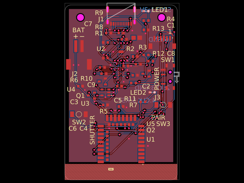 More from this authorAnasSarkiz/magnetic-shutter-remote--01a0f81fA compact USB‑C rechargeable battery device with BQ25185 charging, 3.3‑V regulation and protection, E73 Bluetooth control, temperature monitoring, status/charge LEDs, shutter/pair/power switches, and a mechanically enclosed Li‑Po battery with docking/antenna provisions.
 Similar packagemohan-bee/esp32-c3This hardware design integrates an ESP32-C3 microcontroller, a USB-C connector, a power management IC (AP2112-3.3V regulator), a USB-to-Serial converter (CH340C), several resistors, capacitors, and user-accessible headers to facilitate USB communication, power regulation, and general I/O interfacing.
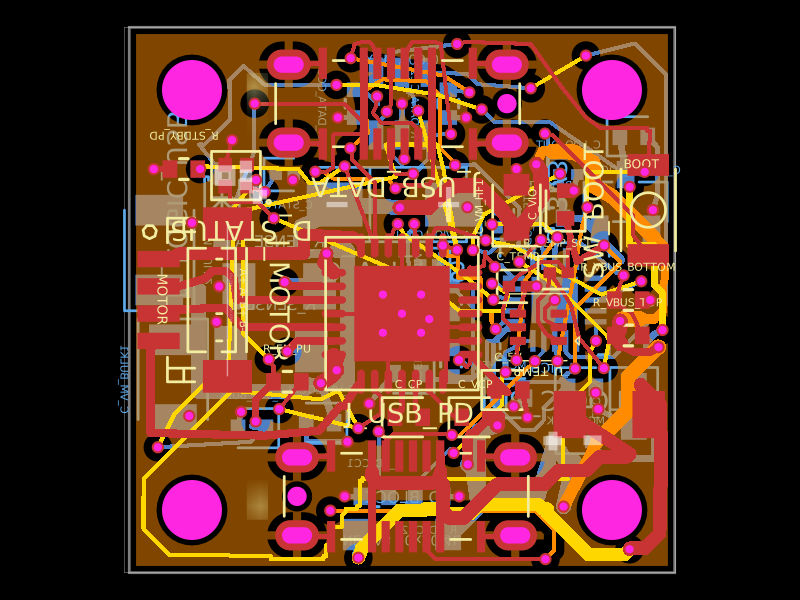 Discover something newShiboSoftwareDev/nema8-20mm-dual-usbc-stepper-controllerA compact 20 mm four-layer USB‑C stepper-controller PCB combining CH32X035 MCU control, TMC2209 motor driving, USB‑C PD/data interfaces, protection/power regulation, temperature/LED status hardware, and NEMA8 motor connectivity.