AnasSarkiz/muse-voice-remote
Muse Voice Remote — bare ESP32-S3R8, 155 TOP JLCPCB parts with real supplier CAD, native 3D assembly and GLB exports. Revised 17 mm case allocation; 0.30 mm via drill /0.45 mm pad. Checked prototype PCB; mechanical, RF and MUSE qualification pending.
- Version
- 1.3.2
- License
- unset
- Stars
- 0
scripts/finish-unrouted.py
#!/usr/bin/env python3
"""Complete KiCad's actual unconnected pairs after FreeRouting.

Use imported pads and existing copper as obstacles, search four copper layers,
and accept each branch only when independent KiCad connectivity improves.
This is a routing finish utility, not a replacement for electrical qualification.
"""
import sys
sys.path.insert(0,"/workspace/.cache/native-python")
import heapq, json, math, os, pathlib, subprocess
import pcbnew
from shapely.geometry import Point, LineString, MultiPoint, Polygon, box
from shapely.ops import unary_union
from shapely.prepared import prep

root=pathlib.Path(__file__).resolve().parents[1]
path=root/"dist/MuseVoiceRemote-library.kicad_pcb"
report_path=root/"dist/native-route-drc.json"
env={**os.environ,"XDG_CONFIG_HOME":"/workspace/.config","XDG_DATA_HOME":"/workspace/.local/share","XDG_CACHE_HOME":"/workspace/.cache"}
layers=[pcbnew.F_Cu,pcbnew.In1_Cu,pcbnew.In2_Cu,pcbnew.B_Cu]
step=0.125; width=0.15; clearance=0.15
via_diameter=0.45; via_drill=0.3
def xy(p):return pcbnew.ToMM(p.x),pcbnew.ToMM(p.y)
def vector(p):return pcbnew.VECTOR2I(pcbnew.FromMM(p[0]),pcbnew.FromMM(p[1]))
def check():
    # Keep actual poured-copper clearance/connectivity current after every edit.
    with (root/"dist/plane-fill-check.log").open("a") as log:
        subprocess.run(["/usr/bin/python3",str(root/"scripts/fill-ground-plane.py"),str(path)],
                       env=env,check=True,stdout=log,stderr=log)
    subprocess.run(["kicad-cli","pcb","drc",str(path),"--format","json","--output",str(report_path)],env=env,check=True,stdout=subprocess.DEVNULL)
    return json.loads(report_path.read_text())
def endpoints(item):
    if isinstance(item,pcbnew.PCB_VIA):return [(xy(item.GetPosition()),i) for i in range(4)]
    if isinstance(item,pcbnew.PCB_TRACK):return [(xy(p),layers.index(item.GetLayer())) for p in [item.GetStart(),item.GetEnd()]]
    return [(xy(item.GetPosition()),i) for i,l in enumerate(layers) if item.GetLayerSet().Contains(l)]
def obstacles(board,net):
    wire=[[] for _ in layers]; via=[]
    for x in [-31.5,31.5]:
        for y in [-22,22]:
            for bucket in wire:bucket.append(Point(x,y).buffer(1.8+width/2))
            via.append(Point(x,y).buffer(1.8+via_diameter/2))
    if net!="GND" and any(z.GetLayer()==pcbnew.In1_Cu and z.GetNetname()=="GND" for z in board.Zones()):
        # Keep an uninterrupted reference beneath RF and crystal copper.
        # Sparse inner-layer signal paths elsewhere are cleared by the zone filler.
        wire[1].append(box(-33,-24,33,24))
    if net not in {"GND","V3_3"} and any(z.GetLayer()==pcbnew.In2_Cu and z.GetNetname()=="V3_3" for z in board.Zones()):
        # General finishing must preserve the supply plane. Existing inner
        # copper remains; new signal paths use top/bottom with legal vias.
        wire[2].append(box(-33,-24,33,24))
    for t in board.GetTracks():
        if isinstance(t,pcbnew.PCB_VIA):
            radius=pcbnew.ToMM(t.GetWidth(pcbnew.F_Cu))/2
            via.append(Point(xy(t.GetPosition())).buffer(radius+via_diameter/2+clearance))
            if t.GetNetname()!=net:
                for bucket in wire:bucket.append(Point(xy(t.GetPosition())).buffer(radius+width/2+clearance))
        elif t.GetNetname()!=net:
            shape=LineString([xy(t.GetStart()),xy(t.GetEnd())])
            r=pcbnew.ToMM(t.GetWidth())/2
            wire[layers.index(t.GetLayer())].append(shape.buffer(r+width/2+clearance))
            via.append(shape.buffer(r+via_diameter/2+clearance))
    for f in board.GetFootprints():
        for p in f.Pads():
            bounds=p.GetBoundingBox();shape=box(*xy(bounds.GetOrigin()),*xy(bounds.GetEnd()))
            copper=p.GetEffectivePolygon(pcbnew.F_Cu)
            if copper.OutlineCount()>0:
                polygons=[]
                for index in range(copper.OutlineCount()):
                    outline=copper.COutline(index)
                    outer=[xy(outline.CPoint(i)) for i in range(outline.PointCount())]
                    holes=[]
                    for h in range(copper.HoleCount(index)):
                        hole=copper.CHole(index,h)
                        holes.append([xy(hole.CPoint(i)) for i in range(hole.PointCount())])
                    polygons.append(Polygon(outer,holes).buffer(0))
                shape=unary_union(polygons)
            if p.GetAttribute()==pcbnew.PAD_ATTRIB_NPTH and f.GetReference() in {"MIC1","MIC2"}:
                # Factory derivative uses 0.50 mm acoustic ports; route against
                # that cutout while retaining the original supplier import.
                shape=Point(xy(p.GetPosition())).buffer(.25)
            # No new via-in-pad holes; retain the original imported thermal holes.
            # Same-net via copper may join a land, but its drill must remain
            # outside the solderable pad. Other nets retain full Cu clearance.
            via.append(shape.buffer(via_drill/2+0.03 if p.GetNetname()==net else via_diameter/2+clearance))
            if p.GetNetname()!=net:
                for i,l in enumerate(layers):
                    if p.GetLayerSet().Contains(l):wire[i].append(shape.buffer(width/2+clearance))
    return [prep(unary_union(b)) for b in wire],prep(unary_union(via))
def route(board,a,b,front_only=False,min_x=None,max_x=None):
    net=a.GetNetname()
    assert net and b.GetNetname()==net
    occupied,via_obstacles=obstacles(board,net)
    connect=board.GetConnectivity()
    via_neighbors={}
    for v in board.GetTracks():
        if not isinstance(v,pcbnew.PCB_VIA) or v.GetNetname()!=net:continue
        for neighbor in list(connect.GetConnectedTracks(v))+list(connect.GetConnectedPads(v)):
            via_neighbors.setdefault(neighbor.m_Uuid.AsString(),[]).append(v)
    def island(item):
        found={};todo=[item]
        while todo:
            current=todo.pop();identifier=current.m_Uuid.AsString()
            if identifier in found or current.GetNetname()!=net:continue
            found[identifier]=current
            todo.extend(connect.GetConnectedTracks(current))
            todo.extend(connect.GetConnectedPads(current))
            todo.extend(via_neighbors.get(identifier,[]))
        return list(found.values())
    def point(n):return n[0]*step,n[1]*step
    def seeds(item):
        result={}
        for connected in island(item):
          for pos,layer in endpoints(connected):
            ix,iy=round(pos[0]/step),round(pos[1]/step)
            for dx in [-1,0,1]:
                for dy in [-1,0,1]:
                    n=(ix+dx,iy+dy,layer);p=point(n)
                    if not occupied[layer].intersects(LineString([pos,p])):result[n]=pos
        return result
    starts,goals=seeds(a),seeds(b)
    def in_bounds(k):return (min_x is None or point(k)[0]>=min_x) and (max_x is None or point(k)[0]<=max_x)
    starts={k:v for k,v in starts.items() if in_bounds(k)}
    goals={k:v for k,v in goals.items() if in_bounds(k)}
    if front_only:
        starts={k:v for k,v in starts.items() if k[2]==0}
        goals={k:v for k,v in goals.items() if k[2]==0}
    if not starts or not goals:raise RuntimeError(f"No clear endpoint for {net}")
    if len(starts)>len(goals):starts,goals=goals,starts
    target_points=MultiPoint(list({point(n) for n in goals}))
    def heuristic(n):return target_points.distance(Point(point(n)))/step
    print(f"Searching {net}: {len(starts)} accessible starts, {len(goals)} goals, {step} mm grid",flush=True)
    queue=[];cost={};prev={};origin={}
    for n,pos in starts.items():
        g=math.dist(pos,point(n))/step;cost[n]=g;origin[n]=pos
        heapq.heappush(queue,(g+heuristic(n),g,n))
    directions=[(1,0),(-1,0),(0,1),(0,-1),(1,1),(1,-1),(-1,1),(-1,-1)]
    cache={}; settled=0
    while queue:
        _,g,n=heapq.heappop(queue)
        if g>cost[n]:continue
        settled+=1
        search_limit = 500000 if net in {"TALK", "STATUS_B", "STATUS_G", "STATUS_R", "BAT", "BL_SENSE", "LCD_BL_ENABLE", "LCD_DC", "USB_EN1", "POWER_GOOD_N"} else 400000 if net=="LCD_LEDA2" else 100000
        if settled>search_limit:raise RuntimeError(f"No clear four-layer route for {net} within search budget; inspect escapes")
        if n in goals:
            nodes=[n]
            while nodes[-1] in prev:nodes.append(prev[nodes[-1]])
            nodes.reverse()
            segments=[(origin[nodes[0]],point(nodes[0]),nodes[0][2])]
            new_vias=set()
            for u,v in zip(nodes,nodes[1:]):
                if u[2]!=v[2]:new_vias.add(point(u))
                else:segments.append((point(u),point(v),u[2]))
            segments.append((point(n),goals[n],n[2]))
            code=a.GetNetCode()
            for p,q,l in segments:
                if math.dist(p,q)<0.000001:continue
                t=pcbnew.PCB_TRACK(board);t.SetStart(vector(p));t.SetEnd(vector(q))
                t.SetLayer(layers[l]);t.SetWidth(pcbnew.FromMM(width));t.SetNetCode(code);board.Add(t)
            for p in new_vias:
                v=pcbnew.PCB_VIA(board);v.SetPosition(vector(p))
                for l in layers:v.SetWidth(l,pcbnew.FromMM(via_diameter))
                v.SetDrill(pcbnew.FromMM(via_drill));v.SetViaType(pcbnew.VIATYPE_THROUGH)
                v.SetLayerPair(pcbnew.F_Cu,pcbnew.B_Cu);v.SetNetCode(code);board.Add(v)
            return len(segments),len(new_vias),settled
        choices=[]
        for dx,dy in directions:
            nxt=(n[0]+dx,n[1]+dy,n[2]);p=point(nxt)
            if abs(p[0])>32.3 or abs(p[1])>23.3:continue
            if not in_bounds(nxt):continue
            key=(n,nxt)
            if key not in cache:cache[key]=occupied[n[2]].intersects(LineString([point(n),p]))
            if not cache[key]:choices.append((nxt,math.hypot(dx,dy)*(1 if n[2]==1 else 1.4)))
        p=point(n)
        if not front_only and abs(p[0])<32.15 and abs(p[1])<23.15 and not via_obstacles.intersects(Point(p)):
            choices.extend(((n[0],n[1],l),2.5/step) for l in range(4) if l!=n[2] and
                           not occupied[l].intersects(Point(p)))
        for nxt,increment in choices:
            new=g+increment
            if new>=cost.get(nxt,float("inf")):continue
            cost[nxt]=new;prev[nxt]=n;origin[nxt]=origin[n]
            heapq.heappush(queue,(new+heuristic(nxt),new,nxt))
    raise RuntimeError(f"No clear four-layer route for {net}")

# A FreeRouting pattern at this connector joins adjacent ground pins using an
# outside U-shaped link that encloses RD. Join the same ground pins directly
# across their adjacent pads so the existing electrical net is preserved and
# the neighboring control pad can escape. No component geometry is changed.
board=pcbnew.LoadBoard(str(path))
connector=next(f for f in board.GetFootprints() if f.GetReference()=="J_LCD")
p31=next(p for p in connector.Pads() if p.GetNumber()=="31")
p32=next(p for p in connector.Pads() if p.GetNumber()=="32")
assert p31.GetNetname()==p32.GetNetname()=="GND"
current_catalog=json.loads((root/"docs/component-catalog.json").read_text())
legacy_te=not any(p["library"].startswith("JLCPCB/") for p in current_catalog)
for horizontal in list(board.GetTracks()) if legacy_te else []:
    if isinstance(horizontal,pcbnew.PCB_VIA) or horizontal.GetNetname()!="GND" or horizontal.GetLayer()!=pcbnew.F_Cu:continue
    a,z=xy(horizontal.GetStart()),xy(horizontal.GetEnd());base=xy(p32.GetPosition())
    if math.dist(a,base)<0.00001:landing=z
    elif math.dist(z,base)<0.00001:landing=a
    else:continue
    if abs(landing[1]-base[1])>0.00001 or abs(landing[0]-base[0])<0.4:continue
    other=(landing[0],xy(p31.GetPosition())[1])
    vertical=next((t for t in board.GetTracks() if not isinstance(t,pcbnew.PCB_VIA) and t.GetNetname()=="GND" and t.GetLayer()==pcbnew.F_Cu and
                   (math.dist(xy(t.GetStart()),landing)<0.00001 and math.dist(xy(t.GetEnd()),other)<0.00001 or
                    math.dist(xy(t.GetEnd()),landing)<0.00001 and math.dist(xy(t.GetStart()),other)<0.00001)),None)
    if vertical is None:continue
    before=path.read_bytes();old=check()
    board.Remove(horizontal);board.Remove(vertical)
    bridge=pcbnew.PCB_TRACK(board);bridge.SetStart(p31.GetPosition());bridge.SetEnd(p32.GetPosition())
    bridge.SetLayer(pcbnew.F_Cu);bridge.SetWidth(pcbnew.FromMM(width));bridge.SetNetCode(p31.GetNetCode());board.Add(bridge)
    pcbnew.SaveBoard(str(path),board);new=check()
    if len(new["unconnected_items"])>len(old["unconnected_items"]) or any(v["type"] not in {"via_dangling","track_dangling"} for v in new["violations"]):
        path.write_bytes(before);raise RuntimeError("Connector ground-link rewrite failed independent checks")
    print("Joined adjacent FPC ground pins directly; freed control-pad escape",flush=True)
    break

deferred_pairs=set()
for iteration in range(512):
    report=check();pending=report["unconnected_items"]
    if not pending:break
    before=path.read_bytes();board=pcbnew.LoadBoard(str(path))
    items={i.m_Uuid.AsString():i for i in list(board.GetTracks())+[p for f in board.GetFootprints() for p in f.Pads()]}
    pending.sort(key=lambda r:({"MIC_WS_HOST":-8,"MIC_BCLK_HOST":-7,"AMP_ENABLE":-6,"AMP_ENABLE_HOST":-6,"SPK_BCLK":-5,"USB_DM_MCU":-4,"HAPTIC":-3,"LCD_2V8":0,"CHG_ITERM":1,"USB_CC2":2,"GND":-10}.get(items[r["items"][0]["uuid"]].GetNetname(),3),
                              math.dist(tuple(r["items"][0]["pos"].values()),tuple(r["items"][1]["pos"].values()))))
    result=None
    for candidate in pending:
        key=tuple(sorted(i["uuid"] for i in candidate["items"]))
        if key in deferred_pairs:continue
        pair=candidate["items"];a,b=[items[p["uuid"]] for p in pair]
        for grid in [0.125,0.05]:
            step=grid
            try:
                result=route(board,a,b)
                break
            except RuntimeError as error:
                if not str(error).startswith(("No clear four-layer route","No clear endpoint")):raise
                print(f"Deferred {a.GetNetname()} at {grid} mm: {error}",flush=True)
        if result is not None:break
        deferred_pairs.add(key)
    if result is None:raise RuntimeError("Remaining nets need local escape repair")
    pcbnew.SaveBoard(str(path),board)
    after=check()
    if len(after["unconnected_items"])>=len(pending) or any(v["type"] not in {"via_dangling","track_dangling"} for v in after["violations"]):
        path.write_bytes(before)
        deferred_pairs.add(key)
        print(f"Independent DRC rejected {a.GetNetname()}; restored previous CAD and deferred this pair",flush=True)
        continue
    print(f"Finished {a.GetNetname()}: {result}; {len(after['unconnected_items'])} pairs remain",flush=True)
else:raise RuntimeError("Unexpected number of remaining branches")

# Copper cleanup is separate: retain and report all intermediate warnings.
final=check()
if final["unconnected_items"] or any(v["type"] not in {"via_dangling","track_dangling"} for v in final["violations"]):
    raise RuntimeError("Connections or geometry still need repair")
print(f"All native pads connected; {len(final['violations'])} redundant-copper flags remain for prune-route-stubs.py",flush=True)
# Avoid KiCad 9 SWIG finalization of detached board-item wrappers.
os._exit(0)
Related Packages
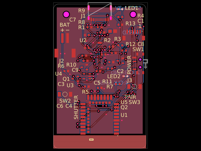 More from this authorAnasSarkiz/magnetic-shutter-remote--01a0f81fA compact USB‑C rechargeable battery device with BQ25185 charging, 3.3‑V regulation and protection, E73 Bluetooth control, temperature monitoring, status/charge LEDs, shutter/pair/power switches, and a mechanically enclosed Li‑Po battery with docking/antenna provisions.
 Similar packagemohan-bee/esp32-c3This hardware design integrates an ESP32-C3 microcontroller, a USB-C connector, a power management IC (AP2112-3.3V regulator), a USB-to-Serial converter (CH340C), several resistors, capacitors, and user-accessible headers to facilitate USB communication, power regulation, and general I/O interfacing.
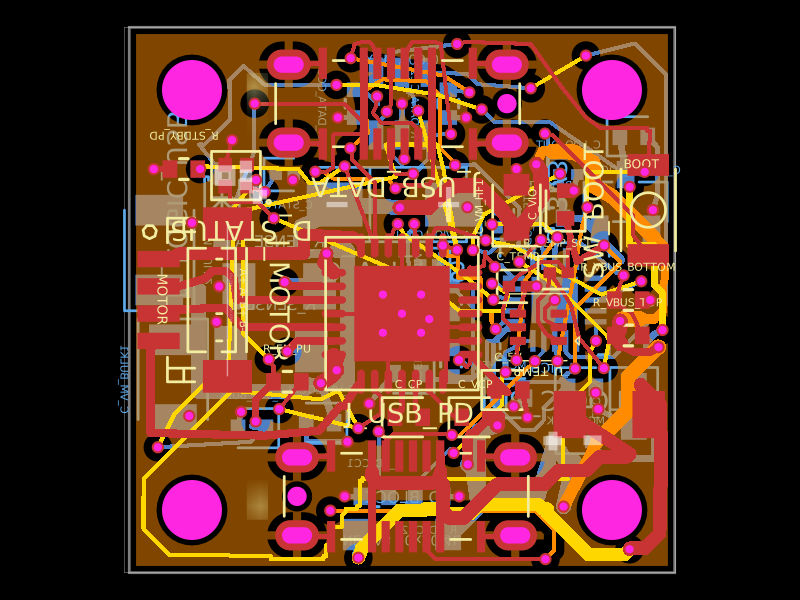 Discover something newShiboSoftwareDev/nema8-20mm-dual-usbc-stepper-controllerA compact 20 mm four-layer USB‑C stepper-controller PCB combining CH32X035 MCU control, TMC2209 motor driving, USB‑C PD/data interfaces, protection/power regulation, temperature/LED status hardware, and NEMA8 motor connectivity.