AnasSarkiz/muse-voice-remote
Muse Voice Remote — bare ESP32-S3R8, 155 TOP JLCPCB parts with real supplier CAD, native 3D assembly and GLB exports. Revised 17 mm case allocation; 0.30 mm via drill /0.45 mm pad. Checked prototype PCB; mechanical, RF and MUSE qualification pending.
- Version
- 1.3.2
- License
- unset
- Stars
- 0
scripts/export-jlcpcb-footprints.py
#!/usr/bin/env python3
"""Convert retained JLCPCB/EasyEDA package records through easyeda2kicad.

No pads are drawn by this script. Library geometry is the supplier import;
native KiCad export is used for independent routing and DRC.
"""
import hashlib
import json
import pathlib
import re
from easyeda2kicad.easyeda.easyeda_importer import EasyedaFootprintImporter
from easyeda2kicad.kicad.export_kicad_footprint import ExporterFootprintKicad

root = pathlib.Path(__file__).resolve().parents[1]
out = root / "vendor/jlcpcb/library"
out.mkdir(parents=True, exist_ok=True)
manifest = []
selection = json.loads((root / "docs/jlcpcb-import-selection.json").read_text())
imports = json.loads((root / "vendor/jlcpcb/import-manifest.json").read_text())
for part in selection["parts"]:
    source = root / f"vendor/jlcpcb/{part['lcsc']}.raweasy.json"
    raw = json.loads(source.read_text())
    for container in [raw, raw["packageDetail"]]:
        if isinstance(container["dataStr"], str):
            container["dataStr"] = json.loads(container["dataStr"])
    imported = EasyedaFootprintImporter(raw).get_footprint()
    target = out / f"{part['lcsc']}.kicad_mod"
    ExporterFootprintKicad(imported).export(str(target), "")
    # EasyEDA HOLE entries are mechanical/non-plated; easyeda2kicad 1.0.1
    # emits empty-number thru_hole pads. Correct the plating metadata while
    # retaining the imported hole positions and diameters exactly.
    text = target.read_text()
    entry = next(e for e in imports["imports"] if e["lcsc"] == part["lcsc"])
    via_pins = entry.get("thermalViaPinBindings", [])
    source_vias = [s.split("~") for s in raw["packageDetail"]["dataStr"]["shape"] if s.startswith("VIA~")]
    if len(source_vias) != len(via_pins):
        raise RuntimeError(f"Unresolved supplier VIA metadata for {part['lcsc']}")
    head = raw["packageDetail"]["dataStr"]["head"]
    thermal = [( (float(v[1])-float(head["x"]))*0.254,
                 (float(v[2])-float(head["y"]))*0.254, b["pin"].removeprefix("pin"))
               for v,b in zip(source_vias,via_pins)]
    corrected_holes = 0
    corrected_thermal = 0
    def classify_empty_pad(match):
        line = match.group(0)
        at = re.search(r'\(at ([\d.-]+) ([\d.-]+)\)',line)
        if not at: raise RuntimeError("Missing imported drill position")
        x,y = map(float,at.groups())
        binding = next((p for p in thermal if abs(p[0]-x)<0.02 and abs(p[1]-y)<0.02),None)
        if binding:
            return line.replace('(pad "" thru_hole',f'(pad "{binding[2]}" thru_hole').replace('*.Paste ', '')
        return line.replace('(pad "" thru_hole','(pad "" np_thru_hole')
    original_empty = re.findall(r'\(pad "" thru_hole[^\n]+',text)
    text = re.sub(r'\(pad "" thru_hole[^\n]+',classify_empty_pad,text)
    corrected_thermal = len(thermal)
    corrected_holes = len(original_empty)-corrected_thermal
    # Filled EasyEDA pad polygons have no edge stroke. The exporter adds a
    # 0.1 mm stroke inside custom-pad primitives, inflating copper by 0.05 mm
    # on each side; remove that exporter artifact to match the original area.
    text, corrected_polygon_strokes = re.subn(
        r'(\(gr_poly\s+\(pts.*?\)\s*)\(width 0\.1\)', r'\1(width 0)', text, flags=re.S)
    # Custom copper polygons are filled regions in the supplier data. KiCad's
    # primitive parser also needs the explicit fill flag (not a zero-width line).
    text, corrected_polygon_fill = re.subn(
        r'(\(gr_poly\s+\(pts.*?\)\s*\(width 0\))\s*\)',
        r'\1 (fill yes)\n\t\t\t)', text, flags=re.S)
    target.write_text(text)
    manifest.append({"library": f"JLCPCB/{part['lcsc']}", "lcsc": part["lcsc"],
                     "mpn": part["mpn"], "file": str(target.relative_to(root)),
                     "sha256": hashlib.sha256(target.read_bytes()).hexdigest(),
                     "source_file": str(source.relative_to(root)),
                     "source_sha256": hashlib.sha256(source.read_bytes()).hexdigest(),
                     "converter": "easyeda2kicad@1.0.1",
                     "nonplated_hole_metadata_corrections": corrected_holes,
                     "plated_thermal_via_metadata_corrections": corrected_thermal,
                     "filled_polygon_stroke_corrections": corrected_polygon_strokes,
                     "filled_polygon_metadata_corrections": corrected_polygon_fill,
                     "physicalPadIds": sorted({str(p.number) for p in imported.pads})})
(root / "vendor/jlcpcb/native-library-manifest.json").write_text(json.dumps(manifest, indent=2) + "\n")
print(f"Converted {len(manifest)} original JLCPCB package footprints; no authored electronic pads.")
Related Packages
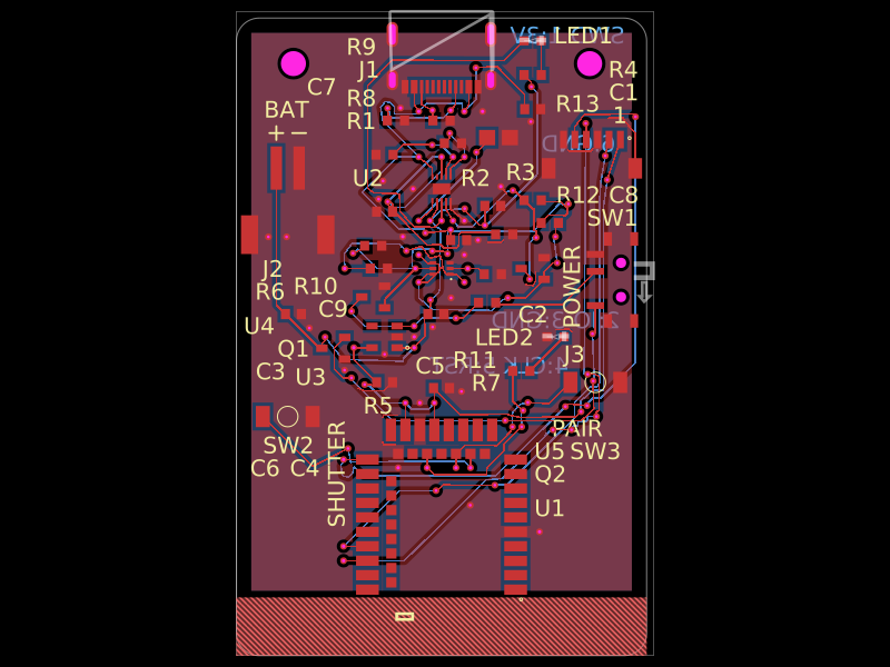 More from this authorAnasSarkiz/magnetic-shutter-remote--01a0f81fA compact USB‑C rechargeable battery device with BQ25185 charging, 3.3‑V regulation and protection, E73 Bluetooth control, temperature monitoring, status/charge LEDs, shutter/pair/power switches, and a mechanically enclosed Li‑Po battery with docking/antenna provisions.
 Similar packagemohan-bee/esp32-c3This hardware design integrates an ESP32-C3 microcontroller, a USB-C connector, a power management IC (AP2112-3.3V regulator), a USB-to-Serial converter (CH340C), several resistors, capacitors, and user-accessible headers to facilitate USB communication, power regulation, and general I/O interfacing.
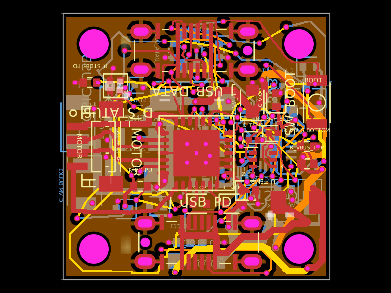 Discover something newShiboSoftwareDev/nema8-20mm-dual-usbc-stepper-controllerA compact 20 mm four-layer USB‑C stepper-controller PCB combining CH32X035 MCU control, TMC2209 motor driving, USB‑C PD/data interfaces, protection/power regulation, temperature/LED status hardware, and NEMA8 motor connectivity.