AnasSarkiz/muse-voice-remote
Muse Voice Remote — bare ESP32-S3R8, 155 TOP JLCPCB parts with real supplier CAD, native 3D assembly and GLB exports. Revised 17 mm case allocation; 0.30 mm via drill /0.45 mm pad. Checked prototype PCB; mechanical, RF and MUSE qualification pending.
- Version
- 1.3.2
- License
- unset
- Stars
- 0
docs/routing.md
# Native routing and fabrication verification

The revised design has 155 populated top-side devices from 56 JLCPCB imports.
Native KiCad CAD preserves their original electronic land patterns, custom pads,
USB plated slots, microphone ports and MCU thermal holes. The board has four
copper layers and four Ø1.8 mm mounting holes. Authoritative final counts,
hashes and native check results belong in `docs/routing-result.json` and
`hardware/drc-report.txt`; historical v1.2.1 counts are not current evidence.

Power/USB routing is deliberately seeded before general signal routing:

- `docs/power-route-seeding.json`: compact top-layer converter and charger
  connections, amplifier bypass and bridge outputs, RF/memory supplies.
- `docs/usb-pair-routing.json`: paired top main paths, duplicate receptacle bridge
  and flow-through ESD connections; main-path mismatch below 0.075 mm.
- `docs/power-plane-seeding.json`: local supply/GND connections, 3.3 V/SYS planes,
  RF/crystal ground patches and ten added ground thermal vias.

L2 is reserved entirely for GND. `save-routed-copper.py` rejects any foreign
signal segment on it. Native filled plane polygons, including every clearance
hole, are preserved as BRep geometry in Circuit JSON. The source-to-pad net map,
placements, rotations, imported hashes and native CAD hash must match before a
normal build will use the copper snapshot.

FreeRouting 2.5.0 / Java 25 handles general routing after the critical seed.
Its DSN clearance reports can differ from native custom-pad/plane geometry;
its success is never accepted as fabrication proof. Actual KiCad connectivity,
clearance, drill, edge and footprint checks decide whether a result is retained.
Native A* and constrained free-space routing utilities finish missing branches.
Each accepted branch must reduce unconnected pairs without introducing geometry
errors. Stub pruning must preserve connectivity. No rule exceptions or waived
errors are used to approve the release.

## Reproduce the checked baseline

```sh
npm ci
npm run check
npm run drc
npm run audit:research
XDG_CONFIG_HOME=/workspace/.config /usr/bin/python3 scripts/export-fabrication.py
```

Normal builds reuse imported components and checked copper; they do not contact
a router. The manufacturing exporter rechecks both logical-reference source CAD
and the factory copy, validates CPL coordinates/rotations/side/count against
KiCad's native position export, and verifies Gerber/drill completeness and ZIP
integrity. It retains original electronic copper while adding only segmented
thermal paste artwork and standard factory reference designators. The supplied
reference map connects them back to the tscircuit source.

## Rerouting changes

Back up working native CAD before rebuilding. `MUSE_ROUTE=preview npm run build`
creates a source/placement preview. Placement is frozen: `place-imported.ts`
requires explicit `--repack`, which invalidates existing routing and requires a
complete reroute. `native-board.py` recreates the board and replaces working Cu.
Do not run either during normal reproduction or over verified routing.

The environment retains KiCad 9/pcbnew, Shapely under
`/workspace/.cache/native-python`, and FreeRouting/Java under
`/workspace/muse-review/tools`. The native finishing scripts operate on
`dist/MuseVoiceRemote-library.kicad_pcb`. Zone filling must use a freshly reloaded
board. Preserve the checked `.kicad_pro` after any board serialization; an
unmatched temporary filename can cause KiCad to write default rules.

After all connections and geometry are clean:

```sh
kicad-cli pcb drc dist/MuseVoiceRemote-library.kicad_pcb \
  --output dist/native-routed-drc.txt --exit-code-violations
/usr/bin/python3 scripts/save-routed-copper.py
npm run check
npm run drc
```

The prototype profile is four layers, 1.0 mm nominal, JLC04101H-3313 stackup,
ENIG, 0.15/0.15 mm tracks/clearance, 0.5 mm copper-to-edge, 0.30 mm minimum via drill / 0.45 mm minimum via pad
and 0.15 mm hole-to-foreign-copper. Nineteen exposed-pad thermal holes require
resin fill/copper cap; microphone NPTH openings remain open. See
`docs/fabrication-notes.md` for the full profile. Controlled RF/USB impedance
requires fabricator confirmation; no measured coupon, RF tuning, physical
assembly or working firmware/MUSE integration is claimed.
Related Packages
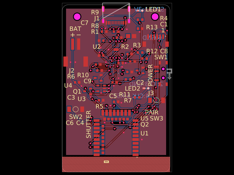 More from this authorAnasSarkiz/magnetic-shutter-remote--01a0f81fA compact USB‑C rechargeable battery device with BQ25185 charging, 3.3‑V regulation and protection, E73 Bluetooth control, temperature monitoring, status/charge LEDs, shutter/pair/power switches, and a mechanically enclosed Li‑Po battery with docking/antenna provisions.
 Similar packagemohan-bee/esp32-c3This hardware design integrates an ESP32-C3 microcontroller, a USB-C connector, a power management IC (AP2112-3.3V regulator), a USB-to-Serial converter (CH340C), several resistors, capacitors, and user-accessible headers to facilitate USB communication, power regulation, and general I/O interfacing.
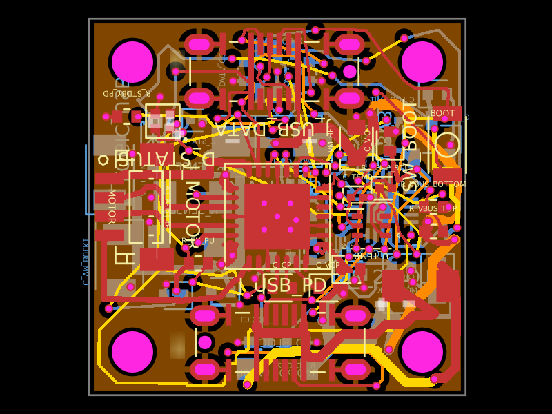 Discover something newShiboSoftwareDev/nema8-20mm-dual-usbc-stepper-controllerA compact 20 mm four-layer USB‑C stepper-controller PCB combining CH32X035 MCU control, TMC2209 motor driving, USB‑C PD/data interfaces, protection/power regulation, temperature/LED status hardware, and NEMA8 motor connectivity.