AnasSarkiz/muse-voice-remote
Muse Voice Remote — bare ESP32-S3R8, 155 TOP JLCPCB parts with real supplier CAD, native 3D assembly and GLB exports. Revised 17 mm case allocation; 0.30 mm via drill /0.45 mm pad. Checked prototype PCB; mechanical, RF and MUSE qualification pending.
- Version
- 1.3.2
- License
- unset
- Stars
- 0
docs/bare-s3.md
# Bare ESP32-S3 chip implementation

U1 is ESP32-S3R8, JLCPCB C2913194, a 7 × 7 mm QFN56 chip with an exposed ground pad and 8 MB in-package Octal PSRAM. It is not a WROOM/MINI carrier module. U_FLASH is a separate W25Q64JVSSIQ (C179171), 8 MB Quad-SPI flash. All active parts import JLCPCB land patterns and retain supplier OBJ/STEP CAD references.

Espressif's ESP32-S3 Datasheet v1.9, Table 1-1, specifies **3.3 V VDD_SPI for ESP32-S3R8**. R8V is a different 1.8 V device and is not selected. VDD_SPI is externally driven from V3_3 through R_VDD_SPI_EXT, a 0 Ω link, using Espressif’s documented external-supply option. The flash has local 0.1 µF/1 µF rail decoupling. Never select the 1.8 V memory configuration or substitute an R8V chip. Six zero-ohm 0402 series positions allow tuning the external flash bus. GPIO33–37 and SPICS1 belong to the in-package PSRAM; they have no external board connections. GPIO45 and GPIO46 have explicit pull-downs for the 3.3 V memory strap and ROM boot conditions. GPIO0 and CHIP_PU retain the BOOT and RESET service controls.

The 40 MHz X322540MPB4SI crystal has 15 pF load capacitance and ±10 ppm initial tolerance. Two 22 pF C0G capacitors assume approximately 4 pF board/device stray capacitance; final values require measured frequency tuning. Espressif's suggested initial 24 nH XTAL_P series inductance is included. RTC, CPU and analog rails have dedicated decoupling; a 2 nH, 900 mA TDK inductor filters VDD3P3 pins 2 and 3.

The RF front end uses an imported Hirose U.FL connector, a CLC matching network and Nexperia low-capacitance ESD protection. Matching values of 1.2 pF / 2 nH / 1.2 pF are initial tuning candidates, not a measured match. RF signal copper stays on the top layer, with a protected inner ground reference beneath the RF and crystal paths. Layer 2 is reserved for GND across the board; the save guard rejects every foreign signal segment on it. Layer 3 also has ground patches beneath RF and the crystal, with a separate 3.3 V plane elsewhere. The target is 50 ohms; the fabricator must establish the actual stackup/trace geometry, and the assembled chip/coax/antenna/enclosure needs RF and harmonic testing.

The supplier footprint contains nine thermal vias within exposed pad 57. Both import adapters preserve their positions, drill sizes and copper, and bind them to the original ground pad. They are plated holes, not non-plated mechanical holes or separate electronic components. The fabrication profile requires resin filling and copper capping for these holes and the ten added power-IC thermal vias, with segmented exposed-pad paste artwork in the separate factory copy.

Microphone word-select uses GPIO41 (physical pin 47, MTDI), an output-capable GPIO matrix signal. The reviewed revision uses GPIO9 (pin 14) for the blue status LED and GPIO6 (pin 11) for TALK; GPIO7 controls charger EN1. GPIO6 is a normal RTC-capable GPIO and is not a ROM UART TX output, so pressing TALK does not short that output. GPIO44/U0RXD controls charger EN2 with a 1 kΩ default pull-down. Firmware must disable the UART0 console before using that pin as a charging control. UART0 TX is unused; native USB programming remains on GPIO19/20. Explicit off-pad control fanout preserves the imported QFN land pattern and routing rules.

Native USB now uses physical QFN pins 25/26 (GPIO19/20); CHIP_PU is pin 4, GPIO0 pin 5, ground pad 57. GPIO15/16 are the XTAL_32K mux pins used as GPIOs because the optional 32 kHz crystal is omitted. GPIO47/48 are the SPICLK_P/N mux pins and remain 3.3 V GPIOs on the selected R8 part.

Manufacturer source snapshots and their commit/hash records are in docs/bare-s3-reference-sources.json and vendor/espressif-bare-s3. The exact ER-TFT028A2-4 interface, two microphones, privacy switch, audio, vibration and charging architecture remain part of the design. Hardware operation, radio performance and the connected MUSE service integration are unverified; the versioned manufacturing package covers prototype PCB/PCBA artwork, with physical qualification still required.
Related Packages
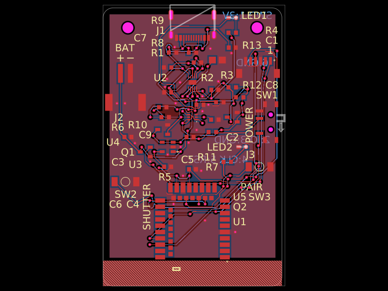 More from this authorAnasSarkiz/magnetic-shutter-remote--01a0f81fA compact USB‑C rechargeable battery device with BQ25185 charging, 3.3‑V regulation and protection, E73 Bluetooth control, temperature monitoring, status/charge LEDs, shutter/pair/power switches, and a mechanically enclosed Li‑Po battery with docking/antenna provisions.
 Similar packagemohan-bee/esp32-c3This hardware design integrates an ESP32-C3 microcontroller, a USB-C connector, a power management IC (AP2112-3.3V regulator), a USB-to-Serial converter (CH340C), several resistors, capacitors, and user-accessible headers to facilitate USB communication, power regulation, and general I/O interfacing.
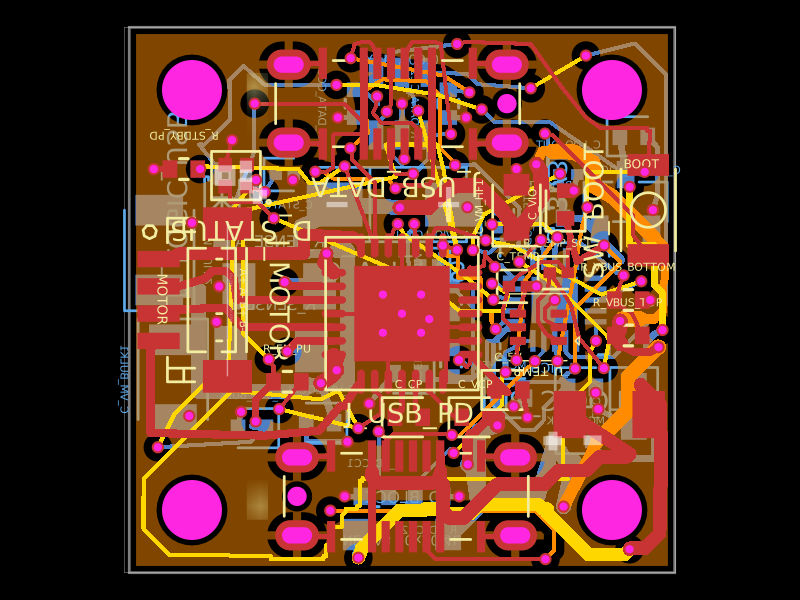 Discover something newShiboSoftwareDev/nema8-20mm-dual-usbc-stepper-controllerA compact 20 mm four-layer USB‑C stepper-controller PCB combining CH32X035 MCU control, TMC2209 motor driving, USB‑C PD/data interfaces, protection/power regulation, temperature/LED status hardware, and NEMA8 motor connectivity.