AnasSarkiz/NEMA14_CH32X035G8U6
A NEMA stepper motor is shown with proposed M3 screws/spacers, four wired motor leads and splices, and a JST SHR-04V-S connector.
- Version
- 1.12.2
- License
- ISC
- Stars
- 0
scripts/repair-routing.py
"""Finish explicitly selected connections on saved copper.
A collision-aware grid assists the selected manual repairs; unchanged routes are retained.
All results must pass the independent tscircuit DRC and Gerber short checks.
"""
import json,math,pathlib,heapq,time
import numpy as np
from PIL import Image,ImageDraw
ROOT=pathlib.Path(__file__).resolve().parents[1];path=ROOT/'artifacts/board.circuit.json';j=json.loads(path.read_text())
STEP=.05;LOW=-17.5;N=701
src={e['source_component_id']:e for e in j if e['type']=='source_component'}
sp={e['source_port_id']:e for e in j if e['type']=='source_port'}
ports={e['pcb_port_id']:e for e in j if e['type']=='pcb_port'}
comp={e['pcb_component_id']:e for e in j if e['type']=='pcb_component'}
nets={e['subcircuit_connectivity_map_key']:e for e in j if e['type']=='source_net'}
traces={e['subcircuit_connectivity_map_key']:e['source_trace_id'] for e in j if e['type']=='source_trace'}
pads=[e for e in j if e['type'] in ['pcb_smtpad','pcb_plated_hole']]
def xy(x,y):return (round((x-LOW)/STEP),round((y-LOW)/STEP))
def world(p):return (LOW+p[0]*STEP,LOW+p[1]*STEP)
def key(e):
 if e['type'] in ['pcb_smtpad','pcb_plated_hole']:
  p=ports.get(e.get('pcb_port_id'),{});return sp.get(p.get('source_port_id'),{}).get('subcircuit_connectivity_map_key')
 return e.get('subcircuit_connectivity_map_key')
def findport(cname,pname):
 return next(p for p in ports.values() if src[comp[p['pcb_component_id']]['source_component_id']]['name']==cname and sp[p['source_port_id']]['name']==pname)
def drawrect(draw,x,y,w,h,r=0):draw.rectangle([xy(x-w/2-r,y-h/2-r),xy(x+w/2+r,y+h/2+r)],fill=1)
def circle(draw,x,y,r):draw.ellipse([xy(x-r,y-r),xy(x+r,y+r)],fill=1)
def obstacle(net,width,via=False):
 imgs=[Image.new('L',(N,N)) for _ in range(2)];ds=[ImageDraw.Draw(i) for i in imgs]
 margin=.15+(.25 if via else width/2)+.018
 for e in j:
  typ=e['type']
  if typ in ['pcb_smtpad','pcb_plated_hole']:
   if key(e)==net and not via:continue
   w=e.get('width',e.get('outer_width',e.get('outer_diameter',e.get('radius',0)*2)));h=e.get('height',e.get('outer_height',e.get('outer_diameter',e.get('radius',0)*2)))
   if abs(e.get('ccw_rotation',0)%180-90)<.01:w,h=h,w
   ls=[0 if l=='top' else 1 for l in e.get('layers',[e.get('layer','top')])]
   for l in ls:drawrect(ds[l],e['x'],e['y'],w,h,margin)
  elif typ=='pcb_trace' and key(e)!=net:
   rr=e['route']
   for a,b in zip(rr,rr[1:]):
    if a['route_type']!='wire' or b['route_type']!='wire' or a['layer']!=b['layer']:continue
    r=margin+max(a['width'],b['width'])/2;d=ds[0 if a['layer']=='top' else 1]
    d.line([xy(a['x'],a['y']),xy(b['x'],b['y'])],fill=1,width=math.ceil(2*r/STEP))
    circle(d,a['x'],a['y'],r);circle(d,b['x'],b['y'],r)
  elif typ=='pcb_via':
   if key(e)==net and not via:continue
   r=.72 if via else e['outer_diameter']/2+margin
   for d in ds:circle(d,e['x'],e['y'],r)
  elif typ=='pcb_keepout':
   c=e['center']
   for d in ds:drawrect(d,c['x'],c['y'],e.get('width',e.get('radius',0)*2),e.get('height',e.get('radius',0)*2),.15+(.25 if via else width/2)+.018)
  elif typ=='pcb_hole':
   for d in ds:circle(d,e['x'],e['y'],e['hole_diameter']/2+.2+(.25 if via else width/2)+.018)
 border=.3+(.25 if via else width/2)
 for d in ds:
  b=math.ceil(border/STEP);d.rectangle([0,0,N-1,b],fill=1);d.rectangle([0,N-1-b,N-1,N-1],fill=1);d.rectangle([0,0,b,N-1],fill=1);d.rectangle([N-1-b,0,N-1,N-1],fill=1)
 return [np.asarray(im,dtype=np.bool_) for im in imgs]
# Move the VM_SENSE bottom-layer diagonal away from the PD_GOOD escape corridor.
removed=next(e for e in j if e.get('pcb_trace_id')=='freerouted_trace_227' and e['type']=='pcb_trace')
assert removed.get('source_net_id')==next(e['source_net_id'] for e in j if e['type']=='source_net' and e['name']=='VM_SENSE')
j.remove(removed)
j[:]=[e for e in j if e.get('pcb_trace_id')!='freerouted_trace_226' and not(e['type']=='pcb_via' and math.hypot(e['x']-3.804,e['y']+1.2898)<.01)]
# Shift the A+ fanout via right/up to open a compliant B+ escape between the two vias.
for e in j:
 if e['type']=='pcb_via' and math.hypot(e['x']-.0359,e['y']+4.5644)<.01:e['x'],e['y']=.45,-4.35
 if e['type']=='pcb_trace':
  for a in e['route']:
   if math.hypot(a['x']-.0359,a['y']+4.5644)<.01:a['x'],a['y']=.45,-4.35
# Remove the redundant leftward A+ fanout jog that obstructed the adjacent B+ escape.
for e in j:
 if e['type']=='pcb_trace' and key(e) in nets and nets[key(e)]['name']=='A_PLUS':
  for a in e['route']:
   if a.get('layer')=='top' and -.01<a['x']<.3 and -5<a['y']<-4:a['x']=.5
# Flip C_VCP so its supply pad faces away from the charge-pump routing pocket.
cc=next(c for c in comp.values() if src[c['source_component_id']]['name']=='C_VCP');cid=cc['pcb_component_id'];cc['rotation']=270
for e in j:
 if e.get('pcb_component_id')==cid and e['type'] in ['pcb_port','pcb_smtpad','pcb_solder_paste']:e['y']=-23.2-e['y']
# Reroute the VCP jog that enclosed the capacitor supply pad.
j[:]=[e for e in j if e.get('pcb_trace_id') not in ['freerouted_trace_277','freerouted_trace_278']]
# Relocate the MCU bypass capacitor to open the voltage-sense escape.
cc=next(c for c in comp.values() if src[c['source_component_id']]['name']=='C_MCU');cid=cc['pcb_component_id']
for e in j:
 if e.get('pcb_component_id')==cid:
  if 'x' in e:e['x']+=.1;e['y']-=1.5
  if 'center' in e:e['center']['x']+=.1;e['center']['y']-=1.5
  if 'anchor_position' in e:e['anchor_position']['x']+=.1;e['anchor_position']['y']-=1.5
  if 'display_offset_x' in e:e['display_offset_x']+=.1;e['display_offset_y']-=1.5
  if 'position' in e:e['position']['x']+=.1;e['position']['y']-=1.5
  for p0 in e.get('route',[]):
   if 'x' in p0:p0['x']+=.1;p0['y']-=1.5
j[:]=[e for e in j if e.get('pcb_trace_id') not in ['freerouted_trace_42','freerouted_trace_201']]
# Move the 3V3 bottom diagonal out of the status-signal escape corridor.
j[:]=[e for e in j if e.get('pcb_trace_id') not in ['freerouted_trace_185','freerouted_trace_234']]
# Reserve three non-crossing top fanouts before routing their bottom continuations.
fanout_records=[]
fanouts={'PD_GOOD':(2.95,-.3),'DATA_PRESENT':(3.2,-1.1),'VM_SENSE':(4.3,-1.9)}
for name,(x,y) in fanouts.items():
 p=findport('U_MCU',name);net=sp[p['source_port_id']]['subcircuit_connectivity_map_key'];tid='manual_fanout_'+name
 bend=(p['x'],y) if name!='PD_GOOD' else (x,p['y'])
 route=[{'route_type':'wire','x':p['x'],'y':p['y'],'layer':'top','width':.16,'start_pcb_port_id':p['pcb_port_id']},{'route_type':'wire','x':bend[0],'y':bend[1],'layer':'top','width':.16},{'route_type':'wire','x':x,'y':y,'layer':'top','width':.16},{'route_type':'via','x':x,'y':y,'from_layer':'top','to_layer':'bottom','via_diameter':.5,'via_hole_diameter':.25},{'route_type':'wire','x':x,'y':y,'layer':'bottom','width':.16}]
 j.append({'type':'pcb_trace','pcb_trace_id':tid,'route':route,'source_net_id':nets[net]['source_net_id'],'source_trace_id':traces[net],'subcircuit_connectivity_map_key':net,'subcircuit_id':'subcircuit_source_group_0','pcb_port_ids':[p['pcb_port_id']]})
 fanout_records.append({'connection':'U_MCU.'+name,'net':name,'route':route,'vias':1,'method':'reserved top fanout'})
 j.append({'type':'pcb_via','pcb_via_id':tid+'_via','pcb_trace_id':tid,'source_trace_id':traces[net],'source_net_id':nets[net]['source_net_id'],'subcircuit_connectivity_map_key':net,'subcircuit_id':'subcircuit_source_group_0','x':x,'y':y,'hole_diameter':.25,'outer_diameter':.5,'layers':['top','bottom']})
repairs=fanout_records
for cname,pname in [('U_MCU','PD_GOOD'),('U_MCU','VM_SENSE'),('U_MCU','DATA_PRESENT'),('U_DRV','OUT2A'),('C_VCP','pin1'),('C_VCP','pin2'),('PATCH','ENABLE_N'),('PATCH','V3V3'),('C_MCU','pin1'),('C_MCU','pin2')]:
 if cname=='PATCH':
  x,y=((5.3187,-2.7939) if pname=='V3V3' else (.4759,-.764));p={'x':x,'y':y,'pcb_port_id':None};net=next(k for k,v in nets.items() if v['name']==pname)
 else:p=findport(cname,pname);net=sp[p['source_port_id']]['subcircuit_connectivity_map_key']
 width=.16
 goals={}
 for e in j:
  if e['type']=='pcb_trace' and key(e)==net and not e['pcb_trace_id'].startswith('manual_fanout'):
   for a in e['route']:
    if a['route_type']=='wire':gx,gy=xy(a['x'],a['y']);goals[(gx,gy,0 if a['layer']=='top' else 1)]=(a['x'],a['y'])
 if not goals:
  for pp in ports.values():
   if pp['pcb_port_id']!=p['pcb_port_id'] and sp[pp['source_port_id']].get('subcircuit_connectivity_map_key')==net:
    gx,gy=xy(pp['x'],pp['y']);goals[(gx,gy,0)]=(pp['x'],pp['y'])
    if any(e.get('pcb_port_id')==pp['pcb_port_id'] and e['type']=='pcb_plated_hole' for e in pads):goals[(gx,gy,1)]=(pp['x'],pp['y'])
 if pname=='VM_SENSE':
  goals={g:v for g,v in goals.items() if math.hypot(v[0]-p['x'],v[1]-p['y'])>2}
 if cname=='PATCH':
  x,y=((2.2473,2.1127) if pname=='V3V3' else (7.1997,-1.3061));gx,gy=xy(x,y);goals={(gx,gy,1):(x,y),(gx,gy,0):(x,y)}
 if cname=='PATCH' and pname=='V3V3':
  goals={}
  for t in j:
   if t.get('pcb_trace_id') in ['freerouted_trace_180','freerouted_trace_184']:
    for a in t['route']:
     gx,gy=xy(a['x'],a['y']);goals[(gx,gy,0 if a['layer']=='top' else 1)]=(a['x'],a['y'])
 if cname=='C_MCU' and pname=='pin1':
  gx,gy=xy(4.675,-2.6267);goals={(gx,gy,0):(4.675,-2.6267)}
 if cname=='C_MCU' and pname=='pin2':
  gx,gy=xy(6.9767,-1.9);goals={(gx,gy,0):(6.9767,-1.9)}
 # Remove the source pad itself from candidate targets.
 goals={g:v for g,v in goals.items() if math.hypot(v[0]-p['x'],v[1]-p['y'])>.25}
 if not goals:raise RuntimeError('No target copper for '+cname+'.'+pname)
 if cname=='U_MCU' and pname in fanouts:
  x,y=fanouts[pname];p={**p,'x':x,'y':y,'pcb_port_id':None}
 blocked=obstacle(net,width);vb=obstacle(net,width,True);start=(*xy(p['x'],p['y']),1 if cname=='PATCH' and pname!='V3V3' or cname=='U_MCU' and pname in fanouts else 0)
 pts=np.asarray([[g[0],g[1],g[2]] for g in goals]);lo=pts[:,:2].min(axis=0);hi=pts[:,:2].max(axis=0)
 def heuristic(s):return max(lo[0]-s[0],0,s[0]-hi[0])+max(lo[1]-s[1],0,s[1]-hi[1])
 heap=[(heuristic(start),0,start)];best={start:0};prev={};end=None;expanded=0
 while heap:
  _,cost,s=heapq.heappop(heap)
  if cost!=best.get(s):continue
  if s in goals:end=s;break
  expanded+=1
  if expanded>600000:break
  x,y,l=s
  options=[(x+dx,y+dy,l,1.41421356 if dx and dy else 1) for dx,dy in [(1,0),(-1,0),(0,1),(0,-1),(1,1),(1,-1),(-1,1),(-1,-1)]]
  if not vb[0][y,x] and not vb[1][y,x]:options.append((x,y,1-l,35))
  for nx,ny,nl,dc in options:
   if not(0<=nx<N and 0<=ny<N) or blocked[nl][ny,nx]:continue
   if nl==l and nx!=x and ny!=y and (blocked[l][y,nx] or blocked[l][ny,x]):continue
   t=(nx,ny,nl);nc=cost+dc
   if nc+1e-8<best.get(t,float('inf')):best[t]=nc;prev[t]=s;heapq.heappush(heap,(nc+heuristic(t),nc,t))
 if end is None:pathlib.Path('/tmp/repair-debug.json').write_text(json.dumps(j));raise RuntimeError(f'No collision-free repair for {cname}.{pname} after {expanded} nodes')
 nodes=[end]
 while nodes[-1]!=start:nodes.append(prev[nodes[-1]])
 nodes.reverse()
 # Retain turns and layer changes; simplify only exact collinear runs.
 slim=[nodes[0]]
 for i in range(1,len(nodes)-1):
  a,b,c=nodes[i-1:i+2]
  if a[2]!=b[2] or b[2]!=c[2] or (b[0]-a[0],b[1]-a[1])!=(c[0]-b[0],c[1]-b[1]):slim.append(b)
 slim.append(nodes[-1]);route=[];newvias=[]
 for i,s in enumerate(slim):
  x,y=world(s);layer='top' if s[2]==0 else 'bottom'
  if i==0:x,y=p['x'],p['y']
  if i==len(slim)-1:x,y=goals[end]
  if route and route[-1]['layer']!=layer:
   old=route[-1]['layer'];route.append({'route_type':'via','x':x,'y':y,'from_layer':old,'to_layer':layer,'via_diameter':.5,'via_hole_diameter':.25})
   newvias.append((x,y))
  route.append({'route_type':'wire','x':x,'y':y,'width':width,'layer':layer})
 if p['pcb_port_id']:route[0]['start_pcb_port_id']=p['pcb_port_id']
 tid=f'manual_repair_{cname}_{pname}'
 j.append({'type':'pcb_trace','pcb_trace_id':tid,'route':route,'source_net_id':nets[net]['source_net_id'],'source_trace_id':traces[net],'subcircuit_connectivity_map_key':net,'subcircuit_id':'subcircuit_source_group_0','pcb_port_ids':[p['pcb_port_id']] if p['pcb_port_id'] else []})
 for i,(x,y) in enumerate(newvias):j.append({'type':'pcb_via','pcb_via_id':tid+'_via'+str(i),'pcb_trace_id':tid,'source_trace_id':traces[net],'source_net_id':nets[net]['source_net_id'],'subcircuit_connectivity_map_key':net,'subcircuit_id':'subcircuit_source_group_0','x':x,'y':y,'hole_diameter':.25,'outer_diameter':.5,'layers':['top','bottom']})
 repairs.append({'connection':cname+'.'+pname,'net':nets[net]['name'],'points':len(route),'vias':len(newvias),'expandedNodes':expanded,'route':route})
 print(repairs[-1]['connection'],nets[net]['name'],len(route),'points',len(newvias),'vias',expanded,'searched nodes',flush=True)
for e in j:
 if e['type']=='pcb_via':e['tented_on_bottom']=True;e['tented_on_top']=True
path.write_text(json.dumps(j,indent=2)+'\n');(ROOT/'artifacts/manual-repairs.json').write_text(json.dumps(repairs,indent=2)+'\n')
Related Packages
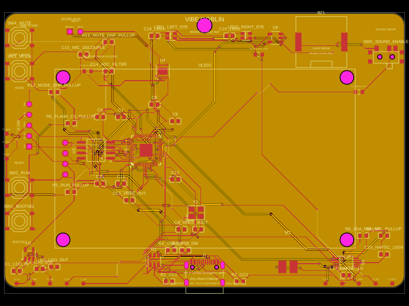 More from this authorAnasSarkiz/vibe_GoblinThese code snippets define various physical electronic components such as ICs, connectors, sensors, LEDs, and chips, specifying their pin layouts, footprint pads, silkscreen markings, courtyard outlines, and 3D CAD models for placement on PCB boards.
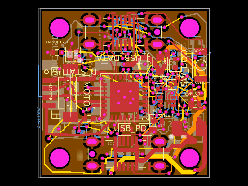 Similar packageShiboSoftwareDev/nema8-20mm-dual-usbc-stepper-controllerA compact 20 mm four-layer USB‑C stepper-controller PCB combining CH32X035 MCU control, TMC2209 motor driving, USB‑C PD/data interfaces, protection/power regulation, temperature/LED status hardware, and NEMA8 motor connectivity.
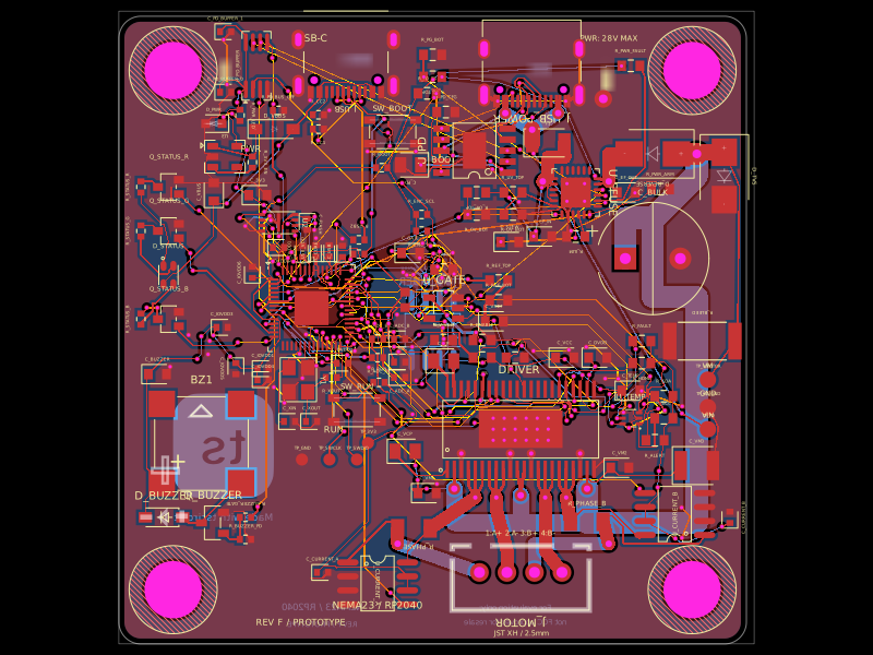 Discover something newimrishabh18/nema-23-stepper-controllerA four-layer NEMA23 stepper motor controller PCB featuring an RP2040 MCU, DRV8452 dual-phase driver, USB‑C PD power input/protection, current and temperature sensing, status LED/buzzer, and optional magnetic encoder.