AnasSarkiz/NEMA14_CH32X035G8U6
A NEMA stepper motor is shown with proposed M3 screws/spacers, four wired motor leads and splices, and a JST SHR-04V-S connector.
- Version
- 1.12.2
- License
- ISC
- Stars
- 0
scripts/package-jlcpcb-review.py
#!/usr/bin/env python3
"""Build the review handoff, including assembly maps and explicit process requests."""
import csv, hashlib, importlib.util, json, pathlib, shutil, zipfile
from html import escape
from shapely.geometry import box
import cairosvg

ROOT=pathlib.Path(__file__).resolve().parents[1]
OUT=ROOT/'artifacts/jlcpcb-review'
spec=importlib.util.spec_from_file_location('cam_audit',ROOT/'scripts/audit-manufacturing.py')
audit=importlib.util.module_from_spec(spec);spec.loader.exec_module(audit)

def svg_geometry(g,color,opacity=1):
    polys=list(g.geoms) if hasattr(g,'geoms') else [g]
    result=[]
    for polygon in polys:
        if polygon.is_empty:continue
        rings=[polygon.exterior]+list(polygon.interiors)
        path=' '.join('M'+' L'.join(f'{x:.5f},{-y:.5f}' for x,y in ring.coords)+' Z' for ring in rings)
        result.append(f'<path d="{path}" fill="{color}" fill-rule="evenodd" opacity="{opacity}"/>')
    return ''.join(result)

def main():
    manifest=json.loads((OUT/'manifest.json').read_text())
    receipt=json.loads((OUT/'order-review-verification.json').read_text())
    assert receipt['prepared_for_JLCPCB_engineering_review']
    assert receipt['native_board_sha256']==hashlib.sha256((ROOT/'artifacts/board.circuit.json').read_bytes()).hexdigest(), 'Review receipt belongs to a different board'
    assert receipt['order_source_sha256']==manifest['order_source_sha256']
    package=json.loads((ROOT/'package.json').read_text())['name']
    j=json.loads((ROOT/'artifacts/board.circuit.json').read_text())
    sources={e['source_component_id']:e for e in j if e['type']=='source_component'}
    parts=sorted([e for e in j if e['type']=='pcb_component'],key=lambda c:sources[c['source_component_id']]['name'])
    thermal=[]
    components={e['pcb_component_id']:e for e in parts}
    for pad in [e for e in j if e['type']=='pcb_smtpad' and e.get('width',0)>1 and e.get('height',0)>1]:
        ref=sources[components[pad['pcb_component_id']]['source_component_id']]['name']
        if ref not in {'U_MCU','U_DRV','U_PD'}:continue
        for via in [e for e in j if e['type']=='pcb_via']:
            if via['pcb_via_id']=='thermal_via_'+ref and audit.shape(pad).covers(audit.shape(via)):
                thermal.append({'Reference':ref,'Via':via['pcb_via_id'],'X mm':via['x'],'Y mm':via['y'],
                                'Drill mm':via['hole_diameter'],'Copper pad mm':via['outer_diameter'],
                                'Process request':'fill, copper cap and planarize; supplier quote and process approval pending'})
    assert len(thermal)==3 and {e['Reference'] for e in thermal}=={'U_MCU','U_DRV','U_PD'}
    with (OUT/'Thermal-Via-Process.csv').open('w',newline='') as f:
        writer=csv.DictWriter(f,fieldnames=list(thermal[0]));writer.writeheader();writer.writerows(thermal)
    joints=[]
    for hole in [e for e in j if e['type']=='pcb_plated_hole']:
        ref=sources[components[hole['pcb_component_id']]['source_component_id']]['name']
        if ref not in {'J_PD','J_DATA','J_MOTOR'}:continue
        joints.append({'Reference':ref,'Pad hints':','.join(hole.get('port_hints',[])),
                       'X mm':hole['x'],'Y mm':hole['y'],
                       'Process request':'approved TOP-side secondary soldering of 0.7 mm USB shell stakes in 1.6 mm PCB; supplier quote/process confirmation pending'})
    assert len([e for e in joints if e['Reference'] in {'J_PD','J_DATA'}])==8
    assert len([e for e in joints if e['Reference']=='J_MOTOR'])==0
    with (OUT/'Through-Hole-Joint-Plan.csv').open('w',newline='') as f:
        writer=csv.DictWriter(f,fieldnames=list(joints[0]));writer.writeheader();writer.writerows(joints)
    for side,prefix in [('top','F'),('bottom','B')]:
        svg=['<svg xmlns="http://www.w3.org/2000/svg" width="1000" height="1000" viewBox="-22 -22 44 44">',
             '<rect x="-22" y="-22" width="44" height="44" fill="white"/>',
             '<rect x="-17.5" y="-17.5" width="35" height="35" fill="#0d4f35"/>']
        mask=audit.gerber(OUT/'cam'/f'{prefix}_Mask.gbr')[0]
        silk=audit.gerber(OUT/'cam'/f'{prefix}_SilkScreen.gbr')[0]
        svg.append(svg_geometry(mask,'#d5b75e'))
        svg.append(svg_geometry(silk,'#ffffff'))
        for e in j:
            if e['type']=='pcb_hole' and e.get('hole_diameter')==3.2:
                svg.append(f'<circle cx="{e["x"]}" cy="{-e["y"]}" r="1.6" fill="white" stroke="#777" stroke-width=".05"/>')
        svg += [f'<text x="0" y="-19.7" text-anchor="middle" font-family="sans-serif" font-size="1">{escape(package)} — {side}</text>',
                '<text x="0" y="20" text-anchor="middle" font-family="sans-serif" font-size=".65">Unmirrored board XY; +Y at top; 35 × 35 mm</text>','</svg>']
        path=OUT/f'{side}-order-preview.svg';path.write_text('\n'.join(svg))
        cairosvg.svg2png(url=str(path),write_to=str(OUT/f'{side}-order-preview.png'))
        # Assembly drawing uses current physical placement centers. Reference
        # captions are a map/table aid; the supplier must approve pickup datums.
        map_svg=svg[:-3]
        for c in parts:
            if c['layer']!=side:continue
            ref=sources[c['source_component_id']]['name'];x,y=c['center']['x'],c['center']['y']
            map_svg.append(f'<rect x="{x-c["width"]/2}" y="{-y-c["height"]/2}" width="{c["width"]}" height="{c["height"]}" fill="none" stroke="#25ccff" stroke-width=".06"/>')
            map_svg.append(f'<text x="{x}" y="{-y}" text-anchor="middle" font-family="sans-serif" font-size=".6" fill="#ff8ddd" stroke="#142238" stroke-width=".08" paint-order="stroke">{escape(ref)}</text>')
        map_svg += ['</svg>'];(OUT/f'{side}-assembly-map.svg').write_text('\n'.join(map_svg))
        paste=audit.gerber(OUT/'cam'/f'{prefix}_Paste.gbr')[0]
        paste_svg='<svg xmlns="http://www.w3.org/2000/svg" width="1000" height="1000" viewBox="-18 -18 36 36"><rect x="-18" y="-18" width="36" height="36" fill="white"/>'+svg_geometry(paste,'black')+'</svg>'
        (OUT/f'{side}-stencil-preview.svg').write_text(paste_svg)
        cairosvg.svg2png(bytestring=paste_svg.encode(),write_to=str(OUT/f'{side}-stencil-preview.png'))
    bottom=', '.join(manifest['bottom_SMT_references']) or 'none'
    mechanical=json.loads((ROOT/'artifacts/mechanical/mount-usb-screen.json').read_text())
    assert mechanical['passed'] and mechanical['board_sha256']==manifest['native_board_sha256']
    instructions=f'''# {package}: JLCPCB engineering review

This handoff is prepared for order review. It is not JLCPCB approval or a production release. No order or payment has been submitted.

Upload `JLCPCB-Gerbers.zip` for the PCB, `JLCPCB-BOM.csv` and `JLCPCB-CPL.csv` for SMT assembly. The BOM contains exact source MPNs and LCSC part numbers. The default `artifacts/nema14-gerbers.zip` applies the same reviewed fabrication and assembly policies. The upstream CLI export is retained under `artifacts/engineering-fixes/upstream-native-gerbers.zip` for diagnosis. `review-cam.zip` contains the exact CAM and detailed source-identity tables used by the independent audit.

Select 4 layers, 35 × 35 mm, 1.6 mm board thickness, and ENIG for the separate bare top-side test-point pads. Request at least 35 um outer copper, 17.5 um inner copper and 20 um plated via barrels. Copper layer order is F_Cu / In1_Cu / In2_Cu / B_Cu. Both drill files are required: plated drills/slots and NPTH. The four mounting holes are Ø3.2 mm at (±13, ±13), with board-center origin.

The 100 um stencil has independently screened fine-pitch apertures and four windows totaling 60% exposed-pad coverage for the MCU, PD controller and A4988. `Thermal-Via-Process.csv` identifies the actual exposed-pad via positions and drill sizes that require filling, copper capping and planarization. Confirm the supplier's paste/reflow and via-in-pad processes before releasing assembly; these capabilities and costs have not been quoted.

SMT fitted parts: {manifest['SMT_components']}. Bottom SMT references: {bottom}. Separate bare top-side `TP_*` test points have no purchased component or stencil paste. JST `J_MOTOR` is native SMT BM04B-SRSS-TB(LF)(SN), C160390, and is included in the top-side SMT BOM and CPL. No bottom-side fitted components or JST through-hole leads are present. The functional order is pin 1 A+, 2 A−, 3 B+, 4 B−. The JST mates vertically from +Z.

The **eight USB-C shell tabs require supplier-approved TOP-side secondary soldering**. Their 0.7 mm stakes do not protrude through the 1.6 mm board; do not assume a bottom-wave or ordinary through-hole process is suitable. `Through-Hole-Joint-Plan.csv` lists the actual eight joint coordinates for supplier quotation or manual soldering. USB signal pads receive stencil paste; shell slots do not. Do not assume an SMT-only quote includes these joints or that the unsoldered USB tabs provide a qualified cable-retention or shield-ground connection.

CPL coordinates are millimeters about board center, unmirrored board XY for both sides. Rotation is the native imported footprint orientation plus component placement rotation. **Check every polarized part and pin 1 in JLCPCB's placement preview.** `placement-orientation-review.json` lists each actual numbered pad, center, side and rotation; source agreement is not proof of supplier pickup convention. Upright USB-C CPL coordinates use the imported land-pattern datum. The CAD body alignment and manufacturer pickup datum are separate conventions; supplier pickup confirmation remains required. Do not substitute a body bounding-box center for the native CPL datum.

The preview images show actual corrected mask and silkscreen Gerbers, not the native CAD captions. Dense silkscreen omits captions that cannot fit safely; all fitted references remain in the assembly maps and placement tables. Inspect assembly maps together with the pad-orientation manifest.

Software verification covers source nets, all saved traces/segments/vias, physical connectivity, actual CAM shorts/opens and clearance, pad/mask/drill agreement, stencil geometry, assembly identities, exact outline and mounts, and nominal native STEP mechanical checks. **USB impedance/reference paths, switching loops, sense/ground return behavior, firmware and thermal performance still require engineering and hardware validation.** A working reference board does not prove this implementation works.

Both upright USB-C sockets occupy opposite edges (+Y and −Y), with cable insertion from +Z. The defined 10 × 7 × 30 mm housings have {mechanical['minimum_simultaneous_plug_gap_mm']:.3f} mm nominal separation. The model screens maximum Ø6 × 3 mm heads within a Ø6.4 mm envelope and an Ø6 mm vertical tool path. Verify actual plugs, fasteners, tool tolerances, JST mating cable, thread engagement and the mounting stack. Rear-motor compatibility has not been verified.

Economic versus Standard PCBA service and panelization are unconfirmed. Require supplier acceptance of the eight short USB shell stakes and the three filled/capped exposed-pad vias before choosing the assembly service. If the accepted service requires a panel, obtain its approved rail, tooling-hole and fiducial requirements; no factory panel is released in this package. Panel/process acceptance is a supplier-review blocker. The functional PCB remains 35 × 35 mm.

Supplier review still must confirm exact stock and quote, pickup orientation, via-in-pad and stencil/reflow process, specified stackup/copper, and assembly sides/THT plan. Do not authorize substitutes. Prototype bring-up must verify USB data, 15 V PD, regulator isolation, phase current/thermal behavior, motor, temperature sensor, LEDs and buzzer before production approval.

Every native and order-source record passes its installed Circuit JSON schema. Display offsets are canonical strings, optional null IDs are omitted, and the buzzer uses a generic pinout record with its real MPN and pin identities retained. See `native-json-compatibility.json`. The actual coupled USB copper and adjacent grounded references are checked separately; fabricator stackup/impedance and bench USB operation remain unverified.

Board source SHA-256: `{manifest['native_board_sha256']}`. Corrected CAM audit: PASS, zero findings. Electrical source, placement, native footprints/courtyards, copper, masks, drills and outline are preserved.
'''
    (OUT/'REVIEW-INSTRUCTIONS.md').write_text(instructions)
    (ROOT/'docs/jlcpcb-order-review.md').write_text(instructions)
    shutil.copy2(ROOT/'artifacts/schematic-a4.pdf',OUT/'schematic-a4.pdf')
    shutil.copy2(OUT/'cam/audit.json',OUT/'CAM-audit.json')
    files=['JLCPCB-Gerbers.zip','JLCPCB-BOM.csv','JLCPCB-CPL.csv','Manual-THT-BOM.csv',
           'Thermal-Via-Process.csv',
           'Through-Hole-Joint-Plan.csv',
           'REVIEW-INSTRUCTIONS.md','manifest.json','order-review-verification.json','order-paste-schema-verification.json','native-json-compatibility.json','CAM-audit.json',
           'placement-orientation-review.json','top-order-preview.svg','bottom-order-preview.svg',
           'top-order-preview.png','bottom-order-preview.png','top-assembly-map.svg','bottom-assembly-map.svg',
           'top-stencil-preview.svg','bottom-stencil-preview.svg','top-stencil-preview.png','bottom-stencil-preview.png',
           'schematic-a4.pdf']
    with zipfile.ZipFile(OUT/'JLCPCB-OrderReview.zip','w',zipfile.ZIP_DEFLATED) as z:
        for name in files:z.write(OUT/name,name)
        for name in ['physical-connectivity.json','reference-feedback/circuit-verification.json','mechanical/mount-usb-screen.json','mount-drill-verification.json']:
            z.write(ROOT/'artifacts'/name,'native-verification/'+name)
    print('Prepared',OUT/'JLCPCB-OrderReview.zip')

if __name__=='__main__':main()
Related Packages
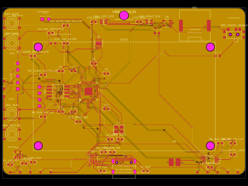 More from this authorAnasSarkiz/vibe_GoblinThese code snippets define various physical electronic components such as ICs, connectors, sensors, LEDs, and chips, specifying their pin layouts, footprint pads, silkscreen markings, courtyard outlines, and 3D CAD models for placement on PCB boards.
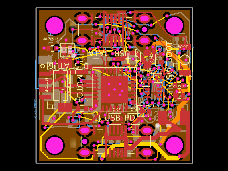 Similar packageShiboSoftwareDev/nema8-20mm-dual-usbc-stepper-controllerA compact 20 mm four-layer USB‑C stepper-controller PCB combining CH32X035 MCU control, TMC2209 motor driving, USB‑C PD/data interfaces, protection/power regulation, temperature/LED status hardware, and NEMA8 motor connectivity.
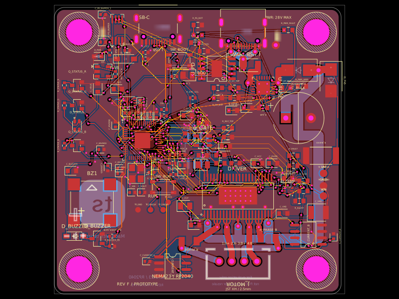 Discover something newimrishabh18/nema-23-stepper-controllerA four-layer NEMA23 stepper motor controller PCB featuring an RP2040 MCU, DRV8452 dual-phase driver, USB‑C PD power input/protection, current and temperature sensing, status LED/buzzer, and optional magnetic encoder.