AnasSarkiz/NEMA14_CH32X035G8U6
A NEMA stepper motor is shown with proposed M3 screws/spacers, four wired motor leads and splices, and a JST SHR-04V-S connector.
- Version
- 1.12.2
- License
- ISC
- Stars
- 0
scripts/audit-manufacturing.py
#!/usr/bin/env python3
"""Independent RS-274X/Excellon audit. No Circuit JSON renderer is used.
Gerbonara 1.5 aperture-rotation and split-line G85 compatibility are explicit.
PyGerber separately renders the original, unmodified Gerbers, including LR.
"""
import argparse,csv,hashlib,importlib.util,json,math,pathlib,re,warnings,zipfile
from collections import Counter,defaultdict
from shapely.geometry import Point,LineString,Polygon,box
from shapely.affinity import rotate
from shapely.ops import unary_union,polygonize
from shapely.strtree import STRtree
from gerbonara import GerberFile,ExcellonFile
from gerbonara.graphic_objects import Flash
from gerbonara.utils import MM
from pygerber.gerberx3.api import v2

def shape(e):
 if e.get('shape')=='polygon':return Polygon([(p['x'],p['y']) for p in e['points']]).buffer(0)
 x,y=e['x'],e['y'];w=e.get('width',e.get('outer_width',e.get('outer_diameter',e.get('radius',0)*2)));h=e.get('height',e.get('outer_height',w))
 if e.get('shape')=='polygon':return Polygon([(p['x'],p['y']) for p in e['points']]).buffer(0)
 if e.get('shape')=='circle' or e['type']=='pcb_via':g=Point(x,y).buffer(w/2,quad_segs=64)
 elif e.get('shape') in ('pill','rotated_pill'):
  dx,dy=((w-h)/2,0) if w>=h else (0,(h-w)/2);g=LineString([(x-dx,y-dy),(x+dx,y+dy)]).buffer(min(w,h)/2,quad_segs=64)
 else:g=box(x-w/2,y-h/2,x+w/2,y+h/2)
 return rotate(g,e.get('ccw_rotation',0),origin=(x,y))
def primitive(p):
 n=type(p).__name__
 if n=='Circle':return Point(p.x,p.y).buffer(p.r,quad_segs=64)
 if n=='Rectangle':return rotate(box(p.x-p.w/2,p.y-p.h/2,p.x+p.w/2,p.y+p.h/2),math.degrees(p.rotation),origin=(p.x,p.y))
 if n=='Line':return LineString([(p.x1,p.y1),(p.x2,p.y2)]).buffer(p.width/2,quad_segs=64)
 if n=='ArcPoly':
  if any(x is not None for x in p.arc_centers):raise ValueError('ArcPoly arc unsupported: explicit failure rather than silent polygon approximation')
  return Polygon(p.outline).buffer(0)
 if n=='Arc':
  r=math.hypot(p.x1-p.cx,p.y1-p.cy);a=math.atan2(p.y1-p.cy,p.x1-p.cx);b=math.atan2(p.y2-p.cy,p.x2-p.cx)
  sweep=((a-b)%(2*math.pi))*(-1) if p.clockwise else (b-a)%(2*math.pi)
  if abs(sweep)<1e-12:sweep=(-1 if p.clockwise else 1)*2*math.pi
  steps=max(8,math.ceil(abs(sweep)*max(r,1)/.001));pts=[(p.cx+r*math.cos(a+sweep*i/steps),p.cy+r*math.sin(a+sweep*i/steps)) for i in range(steps+1)]
  return LineString(pts).buffer(p.width/2,quad_segs=64)
 raise ValueError(f'Unsupported primitive {n}')
def gerber(path):
 raw=path.read_text();rot=0.;angles=[]
 for token in re.findall(r'%[^%]*%|[^*%]+\*',raw):
  m=re.search(r'%LR([+-]?[\d.]+)\*%',token)
  if m:rot=float(m[1]);continue
  if re.search(r'D0?3\*$',token.strip()):angles.append(rot)
 with warnings.catch_warnings(record=True) as ws:
  warnings.simplefilter('always');g=GerberFile.open(path)
 unknown=[str(w.message) for w in ws if not re.search(r'Unknown statement found: \"LR[+\-\d.]+\"',str(w.message))]
 if unknown:raise ValueError(f'{path.name} parser warnings: {unknown}')
 flashes=[o for o in g.objects if isinstance(o,Flash)]
 if len(flashes)!=len(angles):raise ValueError(f'Flash correspondence failure {path.name}: {len(flashes)} / {len(angles)}')
 for o,a in zip(flashes,angles):
  if a%360 not in (0,90,180,270):raise ValueError(f'Rotation {a} requires independently validated analytic support')
  if a%360:o.aperture=o.aperture.rotated(math.radians(a))
 result=Polygon();batch=[];last=True
 for o in g.objects:
  for p in o.to_primitives(unit=MM):
   dark=p.polarity_dark
   if dark!=last and batch:
    u=unary_union(batch);result=result.union(u) if last else result.difference(u);batch=[]
   batch.append(primitive(p));last=dark
 if batch:
  u=unary_union(batch);result=result.union(u) if last else result.difference(u)
 return result,len(g.objects),{'LR_applied':sum(bool(a%360) for a in angles),'warnings':unknown}
def drill(path):
 raw=path.read_text();lines=raw.splitlines();out=[];joined=0
 for l in lines:
  if l.startswith('G85'):
   if not out or not re.fullmatch(r'X[-+\d.]+Y[-+\d.]+',out[-1]):raise ValueError('Ambiguous G85 start')
   start=out.pop();out.extend(['G00'+start,'M15','G01'+l[3:],'M16','G05']);joined+=1;continue
  out.append(l)
 with warnings.catch_warnings(record=True) as ws:
  warnings.simplefilter('always');d=ExcellonFile.from_string('\n'.join(out)+'\n')
 unhandled=[str(w.message) for w in ws if 'G90 header statement found after end of header' not in str(w.message)]
 if unhandled:raise ValueError(f'{path.name} drill warnings: {unhandled}')
 gs=[primitive(p) for o in d.objects for p in o.to_primitives(unit=MM)]
 return unary_union(gs),gs,{'objects':len(d.objects),'G85_joined':joined,'parser_notices':[str(w.message) for w in ws],'tools_mm':dict(Counter(round(o.tool.diameter,6) for o in d.objects))}
def expected(j):
 layers=defaultdict(list)
 for e in j:
  typ=e['type']
  if typ in ('pcb_smtpad','pcb_plated_hole','pcb_via'):
   for l in e.get('layers',[e.get('layer','top')]):layers[l].append(shape(e))
  elif typ=='pcb_trace':
   for a,b in zip(e['route'],e['route'][1:]):
    if a['route_type']==b['route_type']=='wire' and a['layer']==b['layer']:layers[a['layer']].append(LineString([(a['x'],a['y']),(b['x'],b['y'])]).buffer(max(a['width'],b['width'])/2,quad_segs=64))
  elif typ=='pcb_copper_pour':
   q=e['brep_shape'];coords=lambda r:[(p['x'],p['y']) for p in r['vertices']];layers[e['layer']].append(Polygon(coords(q['outer_ring']),[coords(r) for r in q.get('inner_rings',[])]).buffer(0))
 return {k:unary_union(v) for k,v in layers.items()}
def main():
 ap=argparse.ArgumentParser();ap.add_argument('--directory',default='artifacts/manufacturing');ap.add_argument('--source',default='artifacts/board.circuit.json');ap.add_argument('--archive',help='Actual archive to compare byte-for-byte against parsed extracted files');ap.add_argument('--baseline',action='store_true');ap.add_argument('--render',action='store_true');args=ap.parse_args();root=pathlib.Path(__file__).resolve().parents[1];directory=root/args.directory;source_bytes=(root/args.source).read_bytes();j=json.loads(source_bytes);report={'source_sha256':hashlib.sha256(source_bytes).hexdigest(),'directory':args.directory,'parser_versions':{'gerbonara':'1.5.0','pygerber':'2.4.3','shapely':__import__('shapely').__version__},'parser_compatibility':'Only LR right-angle aperture transforms and unambiguous split-line G85 slots are converted to equivalent G00/M15/G01/M16/G05 routing analytically. Original Gerbers independently rendered by PyGerber. Input CAM bytes remain unchanged.','files':{},'issues':[]}
 archive=root/args.archive if args.archive else (root/'artifacts/nema14-gerbers.zip' if args.directory=='artifacts/manufacturing' else directory/'original-export.zip')
 if not archive.exists():raise ValueError(f'Actual archive missing: {archive}')
 archive_records={}
 with zipfile.ZipFile(archive) as z:
  seen=set()
  for member in z.namelist():
   if member.endswith('/'):continue
   name=pathlib.Path(member).name
   if name in seen:raise ValueError(f'Duplicate archive member {name}')
   seen.add(name);data=z.read(member);path=directory/name
   if not path.exists() or path.read_bytes()!=data:raise ValueError(f'Actual archive/extracted byte mismatch: {name}')
   archive_records[name]=hashlib.sha256(data).hexdigest()
 loose_cam={p.name for p in directory.iterdir() if p.suffix in ['.gbr','.drl','.csv']}
 if loose_cam-set(archive_records):raise ValueError(f'Parsed CAM files absent from actual archive: {sorted(loose_cam-set(archive_records))}')
 report['archive']={'path':str(archive),'sha256':hashlib.sha256(archive.read_bytes()).hexdigest(),'extracted_bytes_verified':True,'members':archive_records}
 geo={}
 for p in sorted(directory.glob('*.gbr')):
  geometry,count,compat=gerber(p);geo[p.stem]=geometry;report['files'][p.name]={'sha256':hashlib.sha256(p.read_bytes()).hexdigest(),'objects':count,'area_mm2':geometry.area,'bounds_mm':list(geometry.bounds) if not geometry.is_empty else [],**compat}
  if args.render and p.stem.endswith('_Cu'):
   out=directory/'independent-render';out.mkdir(exist_ok=True);v2.GerberFile.from_file(p).parse(on_parser_error=v2.OnParserErrorEnum.Raise).render_raster(out/(p.stem+'.png'),dpmm=80,color_scheme=v2.ColorScheme.SILK)
 drills=[];all_drill=[]
 for p in sorted(directory.glob('*.drl')):
  g,parts,stats=drill(p);report['files'][p.name]={'sha256':hashlib.sha256(p.read_bytes()).hexdigest(),**stats};all_drill.extend(parts)
  if 'npth' not in p.name:drills.extend(parts)
 holes=unary_union(all_drill);expected_layers=expected(j);layer_names={'top':'F_Cu','bottom':'B_Cu','inner1':'In1_Cu','inner2':'In2_Cu'};actual={};delta={}
 for layer,name in layer_names.items():
  if name not in geo:continue
  a=geo[name].difference(holes);b=expected_layers.get(layer,Polygon()).difference(holes);actual[layer]=a
  missing=b.difference(a.buffer(.0002));extra=a.difference(b.buffer(.0002));delta[layer]={'missing_mm2':missing.area,'extra_mm2':extra.area,'tolerance_mm':.0002}
  if missing.area>1e-4 or extra.area>1e-4:report['issues'].append({'kind':'copper-source-mismatch','layer':layer,**delta[layer]})
 report['copper_comparison']=delta
 # Each connected polygon in the actual copper is an electrical island. Bridge
 # its layers only at drilled plated barrels. Assign names from native pads.
 nodes=[];trees={};indices={}
 for l,g in actual.items():
  ps=list(g.geoms) if hasattr(g,'geoms') else [g];ps=[p for p in ps if p.area>1e-9];indices[l]=list(range(len(nodes),len(nodes)+len(ps)));nodes.extend(ps);trees[l]=STRtree(ps)
 parent=list(range(len(nodes)))
 def find(i):
  while parent[i]!=i:parent[i]=parent[parent[i]];i=parent[i]
  return i
 def union(ids):
  if ids:
   r=find(ids[0])
   for i in ids[1:]:parent[find(i)]=r
 def hits(l,g):return [indices[l][int(i)] for i in trees[l].query(g,predicate='intersects') if nodes[indices[l][int(i)]].intersection(g).area>1e-8]
 for d in drills:
  ann=d.buffer(.03).difference(d.buffer(-.0001));union([i for l in actual for i in hits(l,ann)])
 src={e['source_component_id']:e for e in j if e['type']=='source_component'};pc={e['pcb_component_id']:e for e in j if e['type']=='pcb_component'};sp={e['source_port_id']:e for e in j if e['type']=='source_port'};pp={e['pcb_port_id']:e for e in j if e['type']=='pcb_port'};netnames={e['subcircuit_connectivity_map_key']:e['name'] for e in j if e['type']=='source_net'};assign=defaultdict(lambda:defaultdict(list));netroots=defaultdict(lambda:defaultdict(list));unconnected=[]
 for e in j:
  if e['type'] not in ('pcb_smtpad','pcb_plated_hole') or not e.get('pcb_port_id'):continue
  port=pp[e['pcb_port_id']];s=sp[port['source_port_id']];key=s.get('subcircuit_connectivity_map_key')
  if not key:continue
  ref=src[pc[e['pcb_component_id']]['source_component_id']]['name']+'.'+s['name'];ids=[i for l in e.get('layers',[e.get('layer','top')]) if l in actual for i in hits(l,shape(e).difference(holes))]
  if not ids:unconnected.append(ref)
  for r in {find(i) for i in ids}:assign[r][key].append(ref);netroots[key][r].append(ref)
 shorts=[{'nets':[netnames.get(k,k) for k in v],'pads':dict(v)} for v in assign.values() if len(v)>1];opens=[{'net':netnames.get(k,k),'islands':list(v.values())} for k,v in netroots.items() if len(v)>1];report['connectivity']={'named_nets_checked':len(netroots),'shorts':shorts,'opens':opens,'unconnected_pads':unconnected,'actual_copper_islands':len(nodes),'unassigned_islands':len({find(i) for i in range(len(nodes))}-set(assign))}
 nc_contacts=[]
 for e in j:
  if e['type']!='pcb_smtpad' or not e.get('pcb_port_id'):continue
  port=pp[e['pcb_port_id']];s=sp[port['source_port_id']]
  if s.get('subcircuit_connectivity_map_key'):continue
  for r in {find(i) for i in hits(e['layer'],shape(e))}:
   if r in assign:nc_contacts.append({'pad':src[pc[e['pcb_component_id']]['source_component_id']]['name']+'.'+s['name'],'nets':[netnames.get(k,k) for k in assign[r]]})
 report['connectivity']['no_connect_contacts']=nc_contacts
 if nc_contacts:report['issues'].append({'kind':'no-connect-pad-contact','contacts':nc_contacts})
 # Classify copper islands without named connected pads; expected NC pads
 # must not be mislabeled as floating routed copper.
 isolated=[]
 for r in {find(i) for i in range(len(nodes))}-set(assign):
  geometry=unary_union([nodes[i] for i in range(len(nodes)) if find(i)==r]);nc=[]
  for e in j:
   if e['type']!='pcb_smtpad' or not e.get('pcb_port_id'):continue
   port=pp[e['pcb_port_id']];s=sp[port['source_port_id']]
   if s.get('subcircuit_connectivity_map_key'):continue
   if e['layer'] in actual and r in {find(i) for i in hits(e['layer'],shape(e))}:nc.append(src[pc[e['pcb_component_id']]['source_component_id']]['name']+'.'+s['name'])
  isolated.append({'area_mm2':geometry.area,'bounds_mm':list(geometry.bounds) if not geometry.is_empty else [],'layers':[l for l in indices if any(find(i)==r for i in indices[l])],'no_connect_pads':nc,'classification':'intentional native no-connect pad' if nc else 'unassigned copper: review'})
 report['connectivity']['unassigned_island_details']=isolated
 # Spacing is measured on the independently parsed, finished copper, not on
 # centerlines or bounding rectangles. Same physical barrel-connected nets
 # are exempt; native NC islands remain separate conductors for this screen.
 copper_spacing={}
 for layer,ids in indices.items():
  near=[]
  for local,i in enumerate(ids):
   for other in trees[layer].query(nodes[i].buffer(.5)):
    other=int(other)
    if other<=local:continue
    k=ids[other];ri,rk=find(i),find(k)
    if ri==rk:continue
    ai=set(assign.get(ri,{}));ak=set(assign.get(rk,{}))
    if ai and ai==ak:continue
    distance=nodes[i].distance(nodes[k])
    near.append({'clearance_mm':distance,'conductors':[[netnames.get(n,n) for n in assign.get(r,{})] or ['native NC/unassigned island'] for r in (ri,rk)],'island_indices':[i,k]})
  near.sort(key=lambda e:e['clearance_mm'])
  copper_spacing[layer]={'minimum_distinct_conductor_clearance_mm':near[0]['clearance_mm'] if near else None,'closest_pairs':near[:5],'screen_minimum_mm':.15,'geometry_tolerance_mm':.0002,'scope':'actual finished copper edges; pairs within 0.50 mm; same electrical net excluded'}
  failures=[p for p in near if p['clearance_mm']<.1498]
  if failures:report['issues'].append({'kind':'actual-copper-clearance','layer':layer,'pairs':failures})
 report['actual_copper_spacing']=copper_spacing
 unresolved=[i for i in isolated if not i['no_connect_pads'] and i['area_mm2']>1e-5]
 if unresolved:report['issues'].append({'kind':'unassigned-copper-islands','islands':unresolved})
 if shorts or opens or unconnected:report['issues'].append({'kind':'physical-netlist-failure','short_count':len(shorts),'open_count':len(opens),'unconnected_pads':unconnected})
 bare={s['name'] for s in src.values() if s['ftype']=='simple_test_point'} | {src[p['source_component_id']]['name'] for p in pc.values() if p.get('do_not_place')};bare_pc={p['pcb_component_id'] for p in pc.values() if src[p['source_component_id']]['name'] in bare};bare_pads=unary_union([shape(e) for e in j if e['type']=='pcb_smtpad' and e['pcb_component_id'] in bare_pc]);paste={};pth=unary_union([shape(e) for e in j if e['type']=='pcb_plated_hole'])
 for l in ['F_Paste','B_Paste']:
  bare_pads=unary_union([shape(e) for e in j if e['type']=='pcb_smtpad' and e['pcb_component_id'] in bare_pc and e['layer']==('top' if l=='F_Paste' else 'bottom')])
  g=geo.get(l,Polygon());paste[l]={'bare_interface_overlap_mm2':g.intersection(bare_pads).area,'manual_plated_joint_overlap_mm2':g.intersection(pth).area,'outside_smt_copper_mm2':g.difference(unary_union([shape(e) for e in j if e['type']=='pcb_smtpad' and e['layer']==('top' if l=='F_Paste' else 'bottom')]).buffer(.0002)).area}
  if g.intersection(bare_pads).area>1e-6 or g.intersection(pth).area>1e-6 or paste[l]['outside_smt_copper_mm2']>1e-6:report['issues'].append({'kind':'assembly-paste-policy','layer':l,**paste[l]})
 report['paste']=paste;table={}
 for filename in ['bom.csv','pick_and_place.csv']:
  rows=list(csv.DictReader((directory/filename).open()));refs={r['Designator'] for r in rows};fit={s['name'] for s in src.values() if s['name'] not in bare};table[filename]={'rows':len(rows),'bare_rows':sorted(refs&bare),'missing_fitted':sorted(fit-refs),'unexpected':sorted(refs-fit-bare)}
  duplicates=sorted(ref for ref,count in Counter(r['Designator'] for r in rows).items() if count>1)
  table[filename]['duplicate_refs']=duplicates
  if refs&bare or fit-refs or refs-fit-bare or duplicates:report['issues'].append({'kind':'assembly-table-policy','table':filename,**table[filename]})
  if filename=='bom.csv':
   errors=[]
   byref={e['name']:e for e in src.values()}
   for row in rows:
    component=byref.get(row['Designator'])
    if component is None or row['Designator'] in bare:continue
    mismatch={}
    if row.get('JLCPCB Part #') not in component.get('supplier_part_numbers',{}).get('jlcpcb',[]):mismatch['supplier_part_number']={'export':row.get('JLCPCB Part #'),'source':component.get('supplier_part_numbers',{}).get('jlcpcb',[])}
    if not args.baseline:
     mpn=component.get('manufacturer_part_number');value=component.get('display_resistance',component.get('display_capacitance',mpn))
     for field,expected_value in [('Manufacturer Part Number',mpn),('Comment',mpn),('Value',value)]:
      if not expected_value or row.get(field)!=expected_value:mismatch[field]={'export':row.get(field),'source':expected_value}
    if mismatch:errors.append({'ref':row['Designator'],'errors':mismatch})
   table[filename]['source_identity_errors']=errors
   if errors:report['issues'].append({'kind':'BOM-source-identity','errors':errors})
 report['assembly_tables']=table
 placement_errors=[]
 for row in csv.DictReader((directory/'pick_and_place.csv').open()):
  component=next((e for e in pc.values() if src[e['source_component_id']]['name']==row['Designator']),None)
  if component is None:continue
  errs={}
  for field,val in [('Mid X',component['center']['x']),('Mid Y',component['center']['y']),('Rotation',component.get('rotation',0))]:
   if abs(float(row[field])-val)>.00051:errs[field]={'export':float(row[field]),'source':val}
  if row['Layer'].lower()!=component['layer'].lower():errs['layer']=row['Layer']
  if errs:placement_errors.append({'ref':row['Designator'],'errors':errs})
 report['cpl_coordinate_comparison']={'errors':placement_errors,'origin':'board center; mm; unmirrored top coordinates','rotation':'native imported land-pattern orientation plus saved pcb_component rotation; supplier interpretation still needs placement-preview approval','status':'SOURCE CONVENTION CHECK ONLY; supplier pickup datum and rotation remain USER_REVIEW','USB_centers':[{'reference':src[e['source_component_id']]['name'],'CPL_land_pattern_center_mm':e['center'],'rotation_deg':e.get('rotation',0)} for e in pc.values() if src[e['source_component_id']]['name'] in {'J_PD','J_DATA'}],'USB_center_note':'Upright GCT USB4145 uses native land-pattern CPL datum; local CAD anchor correction X +0.1524952 mm aligns the native STEP centre. Manufacturer pickup datum and JLCPCB placement preview remain unverified.'}
 if placement_errors:report['issues'].append({'kind':'CPL-coordinate-mismatch','errors':placement_errors})
 native_holes=[]
 for e in j:
  if e['type'] not in ('pcb_plated_hole','pcb_via','pcb_hole'):continue
  q=dict(e)
  if e['type']=='pcb_hole':q.update(shape=e.get('hole_shape','circle'),width=e.get('hole_diameter',e.get('hole_width')),height=e.get('hole_diameter',e.get('hole_height')))
  elif e['type']=='pcb_via':q.update(shape='circle',width=e['hole_diameter'],height=e['hole_diameter'])
  else:q.update(width=e.get('hole_width',e.get('hole_diameter')),height=e.get('hole_height',e.get('hole_diameter')))
  native_holes.append(shape(q))
 native_drill=unary_union(native_holes);drill_missing=native_drill.difference(holes.buffer(.00055)).area;drill_extra=holes.difference(native_drill.buffer(.00055)).area
 report['drill_source_comparison']={'missing_mm2':drill_missing,'extra_mm2':drill_extra,'tolerance_mm':.00055,'tolerance_reason':'Exporter slot endpoints and CPL rounded to 3 decimal places; 0.55 micrometer envelope','nominal_mounting_holes':4,'nominal_USB_plated_slots':8}
 if drill_missing>1e-4 or drill_extra>1e-4:report['issues'].append({'kind':'drill-source-mismatch',**report['drill_source_comparison']})
 mask_errors=[]
 for e in j:
  if e['type'] not in ('pcb_smtpad','pcb_plated_hole') or e.get('is_covered_with_solder_mask'):continue
  for l in e.get('layers',[e.get('layer','top')]):
   name={'top':'F_Mask','bottom':'B_Mask'}.get(l)
   if not name:continue
   missing=shape(e).difference(geo[name].buffer(.0002)).area
   if missing>1e-4:mask_errors.append({'id':e.get('pcb_smtpad_id',e.get('pcb_plated_hole_id')),'layer':l,'missing_opening_mm2':missing})
 report['mask_opening_comparison']={'errors':mask_errors,'policy':'uncovered fitted/bare solder pads and plated slots remain open; filled/capped thermal via process required'}
 if mask_errors:report['issues'].append({'kind':'mask-opening-mismatch','errors':mask_errors})
 stencil=[]
 for e in j:
  if e['type']!='pcb_smtpad' or e.get('shape')!='rect' or e.get('width',0)<=2 or e.get('height',0)<=2:continue
  ref=src[pc[e['pcb_component_id']]['source_component_id']]['name']
  if ref in {'U_PD','U_MCU','U_DRV'}:stencil.append({'ref':ref,'pad':e['pcb_smtpad_id'],'coverage_fraction':geo.get('F_Paste',Polygon()).intersection(shape(e)).area/shape(e).area})
 aperture_screen=[]
 for paste_layer in ['F_Paste','B_Paste']:
  geometry=geo.get(paste_layer,Polygon())
  aperture_polygons=list(geometry.geoms) if hasattr(geometry,'geoms') else [geometry]
  for polygon in aperture_polygons:
   if polygon.is_empty:continue
   x1,y1,x2,y2=polygon.bounds;aspect=min(x2-x1,y2-y1)/.1;ratio=polygon.area/(polygon.length*.1)
   aperture_screen.append({'layer':paste_layer,'bounds_mm':list(polygon.bounds),'area_mm2':polygon.area,'perimeter_mm':polygon.length,'aspect_ratio_at_100um':aspect,'area_ratio_at_100um':ratio})
 poor=[e for e in aperture_screen if e['aspect_ratio_at_100um']<1.5-1e-4 or e['area_ratio_at_100um']<.66-1e-4]
 report['stencil_release_screen']={'candidate_thickness_mm':.10,'minimum_aspect_ratio':min((e['aspect_ratio_at_100um'] for e in aperture_screen),default=None),'minimum_area_ratio':min((e['area_ratio_at_100um'] for e in aperture_screen),default=None),'screen_limits':{'aspect_ratio':1.5,'area_ratio':.66},'failing_apertures':poor,'scope':'common geometric release screens only; physical paste/stencil/reflow process acceptance still pending'}
 if poor:report['issues'].append({'kind':'stencil-release-screen','apertures':poor})
 report['exposed_pad_stencil']=stencil
 outline=GerberFile.open(directory/'Edge_Cuts.gbr');segments=[]
 for o in outline.objects:
  for primitive_edge in o.to_primitives(unit=MM):
   if type(primitive_edge).__name__!='Line':raise ValueError('Unexpected outline primitive')
   segments.append(LineString([(primitive_edge.x1,primitive_edge.y1),(primitive_edge.x2,primitive_edge.y2)]))
 outlines=list(polygonize(segments));valid_outline=len(outlines)==1 and abs(outlines[0].area-1225)<1e-6 and outlines[0].bounds==(-17.5,-17.5,17.5,17.5)
 report['board_outline']={'bounds_including_stroke':list(geo['Edge_Cuts'].bounds),'centerline_bounds_mm':list(outlines[0].bounds) if outlines else None,'closed_contour_count':len(outlines),'centerline_length_mm':sum(s.length for s in segments),'centerline_area_mm2':outlines[0].area if outlines else None,'valid_35mm_square':valid_outline}
 if not valid_outline:report['issues'].append({'kind':'outline-failure'})
 measured_webs={}
 for name in ['F_Mask','B_Mask']:
  polygons=list(geo[name].geoms) if hasattr(geo[name],'geoms') else [geo[name]];tree=STRtree(polygons);near=[]
  for i,g in enumerate(polygons):
   for other in tree.query(g.buffer(.25)):
    other=int(other)
    if other>i:near.append(g.distance(polygons[other]))
  minimum=min(near) if near else None;measured_webs[name]={'minimum_web_mm':minimum,'opening_polygons':len(polygons),'scope':'nearest distinct mask openings within 0.25 mm'}
  if not args.baseline and minimum is not None and minimum<.09999:report['issues'].append({'kind':'solder-mask-web','layer':name,'minimum_mm':minimum})
 report['mask_webs']=measured_webs
 report['mask']={n:{'area_mm2':geo[n].area,'bounds_mm':list(geo[n].bounds) if not geo[n].is_empty else []} for n in ['F_Mask','B_Mask'] if n in geo};report['plated_annulus_source_min_mm']=min((min(e.get('outer_width',e.get('outer_diameter',0))-e.get('hole_width',e.get('hole_diameter',0)),e.get('outer_height',e.get('outer_diameter',0))-e.get('hole_height',e.get('hole_diameter',0)))/2 for e in j if e['type'] in ('pcb_plated_hole','pcb_via')),default=None)
 clearances={}
 for l,g in actual.items():
  # Mounting-hole clearance is measured to the physical drill boundary.
  mounts=unary_union([Point(e['x'],e['y']).buffer(e['hole_diameter']/2,quad_segs=64) for e in j if e['type']=='pcb_hole' and e.get('hole_diameter')==3.2])
  clearances[l]={'mount_hole_edge_clearance_mm':g.distance(mounts),'board_edge_clearance_mm':g.distance(box(-18,-18,18,18).difference(box(-17.5,-17.5,17.5,17.5)))}
 report['copper_clearances']=clearances
 keepout_checks=[]
 for e in j:
  if e['type']!='pcb_keepout':continue
  if e.get('shape') not in ('circle','rect'):raise ValueError(f"Unsupported keepout shape: {e.get('shape')}")
  region=shape({**e,'x':e['center']['x'],'y':e['center']['y']})
  for layer in e['layers']:
   if layer not in actual:raise ValueError(f"Declared keepout layer missing from actual CAM: {layer}")
   intrusion=actual[layer].intersection(region).area
   tolerated=actual[layer].intersection(region.buffer(-.0002)).area
   check={'keepout_id':e['pcb_keepout_id'],'shape':e['shape'],'center_mm':e['center'],'layer':layer,'clearance_mm':actual[layer].distance(region),'intrusion_area_mm2':intrusion,'intrusion_beyond_0_0002mm_tolerance_mm2':tolerated}
   keepout_checks.append(check)
   if tolerated>1e-5:report['issues'].append({'kind':'actual-copper-keepout-intrusion',**check})
 report['actual_keepout_checks']=keepout_checks
 silk={}
 for n,m in [('F_SilkScreen','F_Mask'),('B_SilkScreen','B_Mask')]:
  silk[n]={'overlap_mask_openings_mm2':geo[n].intersection(geo[m]).area,'inside_0_15mm_mask_guard_mm2':geo[n].intersection(geo[m].buffer(.1499)).area,'outside_board_0_10mm_inset_mm2':geo[n].difference(box(-17.4,-17.4,17.4,17.4)).area}
  if not args.baseline and (silk[n]['inside_0_15mm_mask_guard_mm2']>1e-5 or silk[n]['outside_board_0_10mm_inset_mm2']>1e-5):report['issues'].append({'kind':'silkscreen-clearance','layer':n,**silk[n]})
 report['silkscreen_clearances']=silk
 if not args.baseline:
  for pane in stencil:
   if abs(pane['coverage_fraction']-.60)>.001:report['issues'].append({'kind':'EP-stencil-coverage',**pane})
  unowned=[e['pcb_solder_paste_id'] for e in j if e['type']=='pcb_solder_paste' and e.get('pcb_component_id') not in pc]
  if unowned:report['issues'].append({'kind':'unowned-source-paste','paste_ids':unowned,'reason':'No component ownership is present in saved source; apertures remain included in full CAM comparison.'})
  comparisons={}
  for source_layer,cam_layer in [('top','F_Paste'),('bottom','B_Paste')]:
   explicit_paste=unary_union([shape(e) for e in j if e['type']=='pcb_solder_paste' and e['layer']==source_layer and (e.get('pcb_component_id') not in pc or src[pc[e['pcb_component_id']]['source_component_id']]['name'] not in bare)])
   actual_paste=geo.get(cam_layer,Polygon())
   comparisons[cam_layer]={'missing_mm2':explicit_paste.difference(actual_paste.buffer(.0002)).area,'extra_mm2':actual_paste.difference(explicit_paste.buffer(.0002)).area}
   if any(v>1e-4 for v in comparisons[cam_layer].values()):report['issues'].append({'kind':'paste-source-mismatch','layer':cam_layer,**comparisons[cam_layer]})
  report['paste_source_comparison']=comparisons
 if (root/args.source).read_bytes()!=source_bytes:raise ValueError('Frozen source changed during independent CAM audit; regenerate and repeat')
 report['status']='FAIL' if report['issues'] else 'PASS';out=directory/'audit.json';out.write_text(json.dumps(report,indent=2,allow_nan=False)+'\n');print(json.dumps({'status':report['status'],'issues':report['issues'],'connectivity':{k:report['connectivity'][k] for k in ['named_nets_checked','actual_copper_islands','unassigned_islands']},'report':str(out)},indent=2));return 0 if args.baseline else bool(report['issues'])
if __name__=='__main__':raise SystemExit(main())
Related Packages
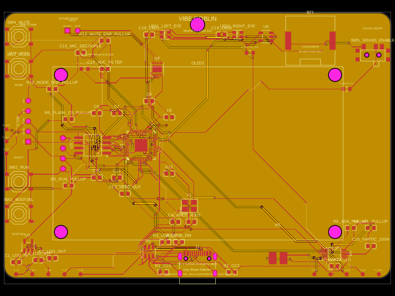 More from this authorAnasSarkiz/vibe_GoblinThese code snippets define various physical electronic components such as ICs, connectors, sensors, LEDs, and chips, specifying their pin layouts, footprint pads, silkscreen markings, courtyard outlines, and 3D CAD models for placement on PCB boards.
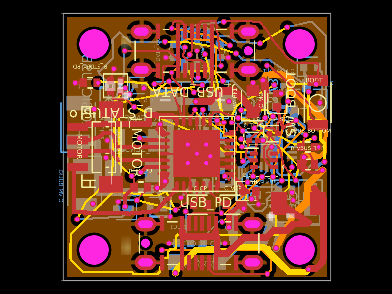 Similar packageShiboSoftwareDev/nema8-20mm-dual-usbc-stepper-controllerA compact 20 mm four-layer USB‑C stepper-controller PCB combining CH32X035 MCU control, TMC2209 motor driving, USB‑C PD/data interfaces, protection/power regulation, temperature/LED status hardware, and NEMA8 motor connectivity.
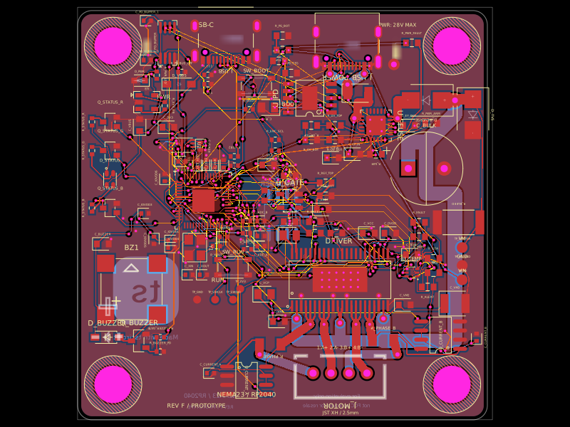 Discover something newimrishabh18/nema-23-stepper-controllerA four-layer NEMA23 stepper motor controller PCB featuring an RP2040 MCU, DRV8452 dual-phase driver, USB‑C PD power input/protection, current and temperature sensing, status LED/buzzer, and optional magnetic encoder.