README.md
# NEMA11 RP2040 routed controller prototype 0.3.0

**Validated development milestone. Not fabrication released.**

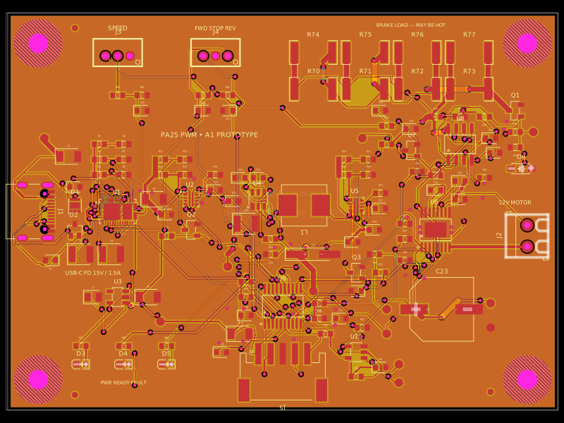
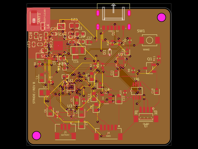
Native tscircuit Circuit JSON contains the routed 35 × 40 mm, four-layer controller,
all 92 electrical components and 341 physical terminals, six functional schematic
sheets, 82 fitted genuine supplier models, the unchanged STEPPERONLINE 11HS12-0674S
motor and an original front-anchored carrier proposal. No rear shaft or mounting
holes are invented. Original 0.1.0 and 0.2.0 source snapshots remain immutable.

The design preserves the exact published NEMA14 v1.13.0 features: RP2040, flash,
crystal, boot/SWD, separate USB-C data and 15 V PD, CH224A/ADC/POWER_GOOD, A4988
and both sense paths, 1/16 microstepping, RGB/power indication, buzzer, temperature,
regulators, protection, test points and optional encoder with both capacitors DNP.
Explicit changes are a 20 kΩ VREF resistor, genuine 1/3 W 0.24 Ω shunts and a
through-hole JST PH header. Manufacturer-required USB locating holes are corrected
in the wrapper while supplier originals remain preserved.

The PCB has 554 traces, 334 vias (minimum 0.45/0.30 mm), 12 component plated holes/
slots and eight NPTH. Independent physical connectivity, shorts, clearances,
clock routing, USB ground reference, every-trace/layer policy and actual CAM
round-trip checks pass. All 36 retained native DRC findings are individually
verified bounding-rectangle approximations of circular keepouts; raw diagnostics
are retained in GitHub. Nine supplier pin metadata warnings remain documented.

The nominal native assembly has no solid interference. All 84 exported model
bounds are independently checked. The original GCT STEP compound's OCCT validity
limitation remains visible. Complete harness, genuine mating plug/contacts and
purchased fasteners are absent. Conditional tool/plug envelopes are procurement
constraints, not physical assembly qualification.

The ideal peak trip is 0.572917 A before routed sense resistance; driver accuracy
at this VREF is not guaranteed. Factory-approved stackup/90 Ω USB impedance,
1 oz on every layer, actual PCB thickness ≤1.60 mm or JST acceptance, filled/capped
vias, stencil, panel/assembly process, stock, wire insulation OD/crimp qualification,
current/thermal/regeneration and physical operation remain unresolved. Do not order
this milestone as a released production assembly.

Open with `tsci dev index.circuit.json`; build with `tsci build index.circuit.json`.
The canonical source and exact review Gerbers, 81-placement JLC SMT BOM/CPL,
manual assembly list, six-page A4 PDF, native GLBs and independent reports are in
[NEMA11_RP2040](https://github.com/AnasSarkiz/NEMA11_RP2040).
See [manufacturing requirements](https://github.com/AnasSarkiz/NEMA11_RP2040/blob/main/docs/manufacturing-requirements.md).
`package-verification.json` is the pre-upload source receipt; GitHub publication
artifacts independently verify the uploaded bytes.