0hmX/bluetooth-pedometer-pcb
This code defines and renders a detailed electronic circuit board layout with labeled components, footprints, 3D models, and routing, suited for PCB design and manufacturing.
- Version
- 1.0.4
- License
- unset
- Stars
- 0
docs/validation.md
# Validation Record

Validation date: **2026-09-04**

## Passed checks

| Check | Result |
| --- | --- |
| `bun run typecheck` | Passed |
| `bunx tsci check netlist` | 0 errors, 0 warnings |
| `bunx tsci check schematic-placement index.circuit.tsx` | Passed with 0 findings |
| `bunx tsci check placement` | 0 placement issues |
| `bunx tsci check shorts index.circuit.tsx` | Passed after reducing the complete VBUS net to 0.2 mm; no Gerber-level shorts detected |
| Build routing | 139 routed traces, zero autorouter connection failures |
| Visual generation | PCB, schematic, and 3D PNGs generated and inspected |

## Findings that remain open

The build produces two routing-clearance errors at the configured 0.08 mm minimum:

1. A STATUS_LED via is 0.053 mm from the V3_3 trace between C13 and U1 VDDD.
2. The ACCEL_INT via is 0.032 mm from the unused BMA400 INT2 pad.

These are not shorts in the Gerber bitmap checker, but they violate the design clearance and must be rerouted before release. Do not lower the rule merely to make the report green.

Additional findings:

- The general build emits an orientation heuristic for J1 even though the USB-C receptacle is intentionally placed at the bottom edge with its mating opening outward.
- `routing-difficulty` reports a maximum estimated failure probability of 18.8% around U2.
- RF_MCU total analyzed length is 8.00 mm; the MCU-to-match branch is 3.84 mm against its 4 mm constraint.
- RF_ANT total analyzed length is 6.16 mm; the antenna branch is 2.16 mm against its 8 mm constraint.
- X48P total analyzed length is 6.73 mm. X48N total is 8.90 mm, while its constrained endpoint path is 5.99 mm. The build still emits one aggregate 8 mm trace-length warning.
- X32P and X32N aggregate analyzed lengths are 12.36 mm and 12.68 mm because each net also includes a load-capacitor branch; the MCU-to-crystal paths are 5.98 mm and 6.15 mm.
- Generic passive land patterns trigger copper-overlap warnings against their selected LCSC footprints. The exact production land patterns need to be normalized before release.
- The exact imported Y2 crystal and Q1 MOSFET wrappers retain supplier pin/footprint data but currently use generic chip semantics, which produces source pin-metadata warnings. Convert or explicitly review those wrappers before release.
- STEP export completed, but the converter could not merge several supplier STEP models. The resulting file is incomplete as a component-level mechanical model.

## Generated outputs

`dist/manufacturing/` contains:

- Gerber ZIP
- preliminary JLCPCB BOM and component-placement CSV
- schematic PDF/SVG
- PCB and assembly SVG
- readable netlist
- KiCad project ZIP
- partial STEP assembly

These outputs are for review only until `pre-order-checklist.md` is complete.
Related Packages
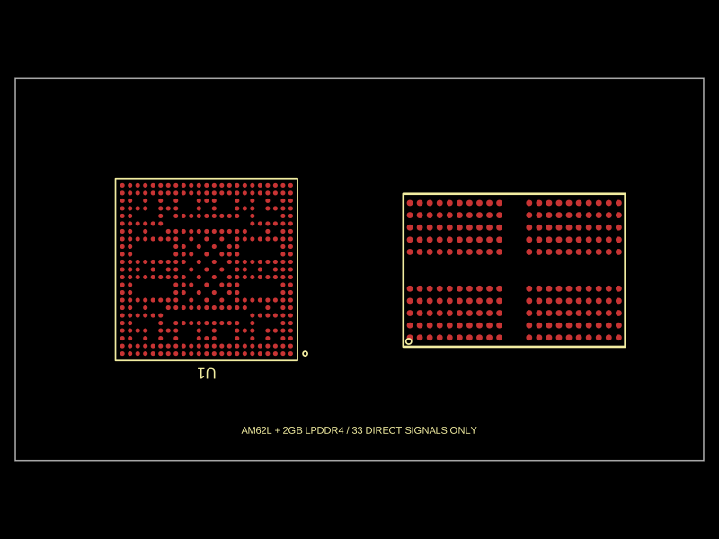 More from this author0hmX/simplified-am62l-computerThis code defines components and scripts for physically representing and routing high-speed DDR memory signals, power lines, and ground planes on an 8-layer PCB with detailed pin assignments, copper pours, and precise via and trace layouts based on TI EVM reference data.
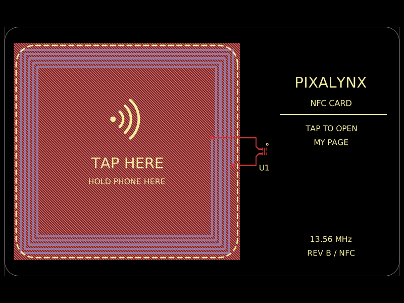 Similar packagepixalynx/pixal-nfc-cardThis code defines React components representing specific electronic hardware components—namely, a 100-ohm SMD resistor, a surface-mount LED, and a chip with labeled pins—each modeled with detailed footprints, 3D CAD models, and manufacturer part information for PCB design.
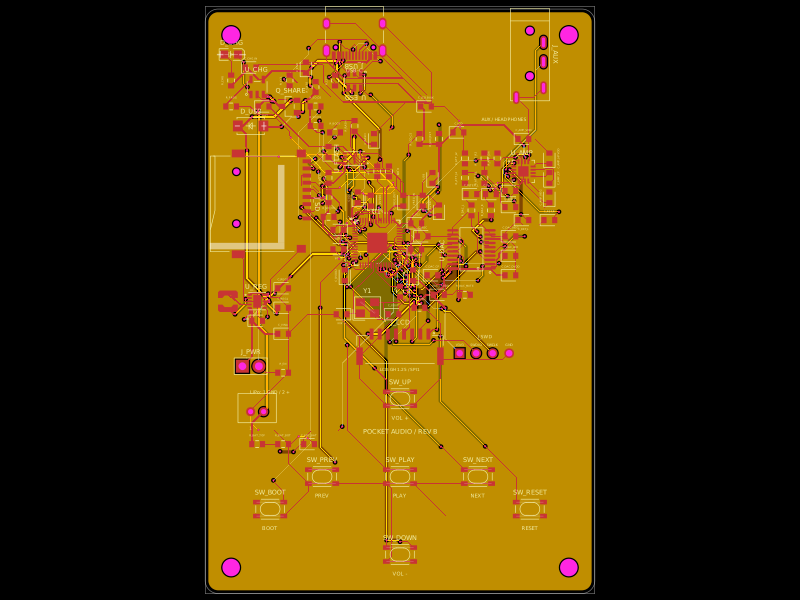 Discover something newDevesh36/pocket-audio-playerA portable, rechargeable microSD audio player built around an RP2040, SPI flash, USB‑C charging/power management, LCD/button controls, PCM5102A I²S DAC, and TPA6132A headphone amplifier in a 3D‑printed enclosure.