0hmX/bluetooth-pedometer-pcb
This code defines and renders a detailed electronic circuit board layout with labeled components, footprints, 3D models, and routing, suited for PCB design and manufacturing.
- Version
- 1.0.4
- License
- unset
- Stars
- 0
docs/pre-order-checklist.md
# Pre-order Checklist

This board is **not order-ready** until every hard gate below is closed and the resulting files are regenerated.

## Hard gates

- [ ] Freeze maximum board dimensions, outline, mounting method, connector access, keepouts, and enclosure materials.
- [ ] Select the exact protected battery; verify capacity, dimensions, protection, NTC curve, connector family, polarity, and three-wire pin order.
- [ ] Select the exact 3.3 V OLED module and cable; verify GND/3V3/SCL/SDA order, I2C address, pull-ups, inrush, and off-state back-powering.
- [ ] Resolve both PCB clearance errors recorded in `validation.md`, then rebuild with zero circuit-JSON routing errors.
- [ ] Replace or explicitly approve every generic passive footprint whose copper differs from the selected LCSC land pattern.
- [ ] Review the BQ27427 DSBGA fanout and via-in-pad process with JLCPCB; obtain a compatible stackup/process quote.
- [ ] Re-place/reroute the 32.768 kHz and 48 MHz crystal networks using the oscillator guidance and close the remaining trace-length warning.
- [ ] Convert the RF feed to the selected JLC stackup's controlled-impedance geometry and validate the antenna keepout/tuning in the final enclosure.
- [ ] Correct the schematic-placement warnings and perform an independent electrical/ERC review.
- [ ] Confirm charger resistor selections and battery temperature thresholds against the selected cell.
- [ ] Review USB-C, IC, diode, MOSFET, crystal, antenna, and connector pin-1/polarity orientations in JLCPCB's placement preview.
- [ ] Verify the generated CPL rotations against JLC's component-orientation convention. The current CSV contains design rotations and is preliminary.
- [ ] Inspect Gerber copper, mask, paste, drill, outline, and copper-to-edge rules in an independent CAM viewer.
- [ ] Re-run `bun run typecheck`, the full check sequence, and `bun run build:release`; record zero unintended shorts.
- [ ] Regenerate Gerbers, BOM, CPL, schematic, assembly drawing, and mechanical model from the final source and checksum/archive that exact release.

## Manufacturing review

- [ ] Confirm 4-layer, 1.0 mm board thickness, copper weights, surface finish, mask color, controlled impedance, smallest trace/space, and drill/via capability with JLCPCB.
- [ ] Confirm exposed-pad paste reduction/thermal-via strategy for U1 and U2.
- [ ] Confirm stencil and assembly support for 0201 RF parts, the BQ27427 DSBGA, and via-in-pad structures.
- [ ] Check basic/extended part fees, minimum order quantities, attrition, and live stock immediately before checkout.
- [ ] Add battery, OLED, cables, and fixture items to the purchasing BOM.
- [ ] Review the STEP export warning: several downloaded component STEP models could not be merged, so use the 3D PNG and original vendor models for mechanical verification.

## Prototype release and test

- [ ] Order a small engineering quantity only after the hard gates pass.
- [ ] Assemble at least one board without battery/OLED and use current-limited bench bring-up.
- [ ] Validate SWD programming/recovery, both clocks, I2C devices, charger states, fuel-gauge current sign, OLED gating, button behavior, BLE range, and sleep current.
- [ ] Measure real battery life and thermal behavior before any larger build.
Related Packages
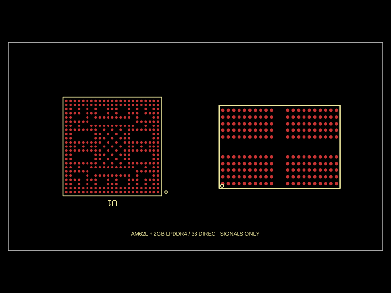 More from this author0hmX/simplified-am62l-computerThis code defines components and scripts for physically representing and routing high-speed DDR memory signals, power lines, and ground planes on an 8-layer PCB with detailed pin assignments, copper pours, and precise via and trace layouts based on TI EVM reference data.
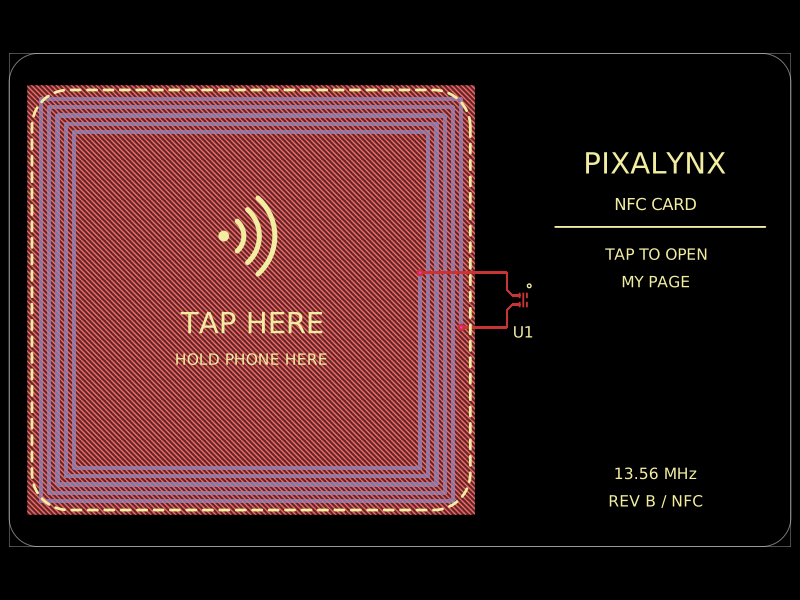 Similar packagepixalynx/pixal-nfc-cardThis code defines React components representing specific electronic hardware components—namely, a 100-ohm SMD resistor, a surface-mount LED, and a chip with labeled pins—each modeled with detailed footprints, 3D CAD models, and manufacturer part information for PCB design.
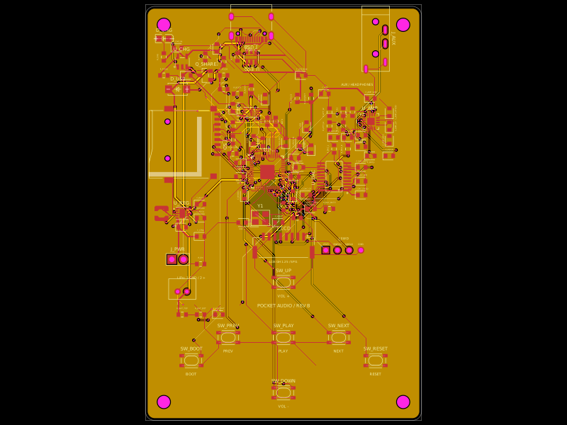 Discover something newDevesh36/pocket-audio-playerA portable, rechargeable microSD audio player built around an RP2040, SPI flash, USB‑C charging/power management, LCD/button controls, PCM5102A I²S DAC, and TPA6132A headphone amplifier in a 3D‑printed enclosure.