0hmX/bluetooth-pedometer-pcb
This code defines and renders a detailed electronic circuit board layout with labeled components, footprints, 3D models, and routing, suited for PCB design and manufacturing.
- Version
- 1.0.4
- License
- unset
- Stars
- 0
docs/bringup.md
# Firmware and Hardware Bring-up

## Before applying power

1. Inspect USB-C, U2, U3, U1, U5, crystals, RF components, and all exposed pads under magnification. Confirm pin-1 orientation against the primary package drawings.
2. Measure resistance from VBUS, SYS/PMID, VBAT_SYS, V3_3, and OLED_3V3 to ground. Investigate a low or unstable reading before power is applied.
3. Keep the OLED and battery disconnected for the first power-up.
4. Power VBUS from a current-limited 5 V bench source, initially limited to 20 mA. Increase the limit only after checking for heating and verifying that V3_3 regulates correctly.

## Test pads

| Pad | Signal | Use |
| --- | --- | --- |
| TP1 | GND | Debug/programming reference |
| TP2 | V3_3 | Rail measurement and target-voltage sense; do not back-power casually |
| TP3 | SWDIO | ARM SWD data |
| TP4 | SWCLK | ARM SWD clock |
| TP5 | RESET | Active-low device reset |
| TP6 | DISPLAY_EN_N | Active-low OLED-rail control and measurement |

Use a TI-supported CC23xx SWD probe and keep pogo leads short. Verify the probe's target-voltage setting before connecting it.

## First firmware image

1. Program a minimal image that leaves `DISPLAY_EN_N` high/high-impedance, disables the status LED, and exposes a low-rate serial/logging path through the debugger.
2. Confirm reset recovery and repeatable erase/program/verify cycles.
3. Verify the 48 MHz and 32.768 kHz oscillator startup. If the low-frequency crystal is not stable, use the supported internal oscillator temporarily and inspect component values/layout before continuing.
4. Scan I2C at 100 kHz. Expected addresses are BMA400 `0x14` with SDO tied low and BQ27427 `0x55`. The OLED address is module-dependent and must not be assumed until the module is selected.
5. Read BMA400 identity/status, configure its low-power step/activity mode, then verify INT1 transitions at DIO11.
6. Initialize the BQ27427 only after selecting the battery chemistry/profile and capacity. Confirm voltage, current sign, state of charge, and GPOUT behavior through charge and discharge.
7. Read BQ25185 STAT1/STAT2 at DIO13/DIO12 and compare them with the charger state table. The charger has no I2C interface in this revision.
8. Pull `DISPLAY_EN_N` low briefly, verify OLED_3V3 and inrush, then initialize the selected OLED. Return the pin high before entering sleep.
9. Exercise BLE advertising, connection, notification, and recovery while watching V3_3 and RF behavior.

## Button behavior

SW1 is connected to the BQ25185 TS/MR node in parallel with the battery thermistor connection. Firmware should not treat it as an ordinary MCU GPIO. Short and long presses can affect charger/reset/ship-mode behavior; validate the exact timing from the BQ25185 data sheet with the selected thermistor and battery attached.

## Power and runtime validation

- Measure board current with the OLED rail off in reset, idle, standby, sensor step mode, advertising, and connected states.
- Capture average and peak current across at least 60 seconds; a multimeter alone can miss radio/display peaks.
- Confirm the OLED rail falls close to 0 V when off and that module pull-ups do not back-power it through SDA/SCL.
- Run a full charge/discharge cycle to validate BQ27427 learning/configuration and charger termination.
- Recalculate the budget in `architecture.md` using measured currents and the selected cell's tested usable capacity.

## RF checks

Start with conducted or shield-box checks if available. At minimum, compare advertising range and packet error rate in the intended enclosure with the battery and display cable installed. Do not tune the matching network from RSSI alone; use an RF fixture/VNA or qualified lab support.
Related Packages
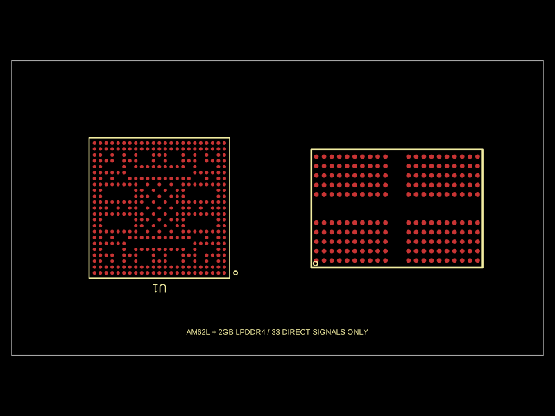 More from this author0hmX/simplified-am62l-computerThis code defines components and scripts for physically representing and routing high-speed DDR memory signals, power lines, and ground planes on an 8-layer PCB with detailed pin assignments, copper pours, and precise via and trace layouts based on TI EVM reference data.
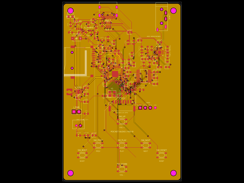
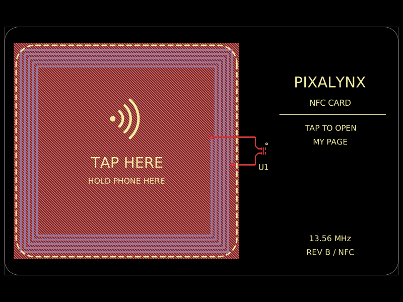 Similar packagepixalynx/pixal-nfc-cardThis code defines React components representing specific electronic hardware components—namely, a 100-ohm SMD resistor, a surface-mount LED, and a chip with labeled pins—each modeled with detailed footprints, 3D CAD models, and manufacturer part information for PCB design.
 Discover something newDevesh36/pocket-audio-playerA portable, rechargeable microSD audio player built around an RP2040, SPI flash, USB‑C charging/power management, LCD/button controls, PCM5102A I²S DAC, and TPA6132A headphone amplifier in a 3D‑printed enclosure.