0hmX/bluetooth-pedometer-pcb
This code defines and renders a detailed electronic circuit board layout with labeled components, footprints, 3D models, and routing, suited for PCB design and manufacturing.
- Version
- 1.0.4
- License
- unset
- Stars
- 0
docs/architecture.md
# Bluetooth Pedometer Architecture

## Status

This is a reviewable first-spin design package, not an order-approved release. The electrical architecture, exact assembled parts, schematic, placement, routing, previews, and preliminary fabrication outputs exist. The gates listed in `pre-order-checklist.md` still need to be closed.

## Frozen design assumptions

These choices were necessary to make progress because the product mechanics and accessories were not supplied.

| Item | Design assumption |
| --- | --- |
| PCB | 46 mm × 32 mm, 1.0 mm thick, rounded rectangle, four copper layers |
| Battery | Protected 1-cell Li-ion/Li-polymer pack, nominal 100 mAh, 4.2 V charge termination |
| Battery cable | Three conductors: PACK+, 10 kΩ NTC/MR, PACK−; JST-PH board header |
| Charging | USB-C 5 V sink, 5.1 kΩ CC resistors, approximately 50 mA charge current and 100 mA input limit |
| Display | External 3.3 V SSD1306-style I2C OLED module connected through a four-pin JST-SH cable |
| User input | One tactile button shared with the charger's TS/MR function |
| Debug | Six labeled pogo/test pads for ground, 3.3 V, SWDIO, SWCLK, reset, and display-enable-not |
| RF | Johanson 2450AT18A100E chip antenna with the TI CC2340R5 RGE matching topology and a four-layer keepout |

The exact battery pack, cable pinout, OLED module, enclosure, mounting method, and antenna environment are not frozen. Those assumptions are therefore pre-order blockers.

## Functional architecture

```text
USB-C 5 V -> BQ25185 charger/power path -> SYS/PMID -> TPS7A02 3.3 V -> CC2340R5
                         |                    |                    -> BMA400
                         |                    |                    -> BQ27427 VDD
                         |                    `-> AO3401A switch -> external OLED
                         |
protected Li-ion PACK+ -> BQ27427 internal sense resistor -> charger BAT/system
```

The BQ27427 is in the battery's high-side current path: `BAT` Kelvin-senses PACK+ and `SRX` feeds the charger/system side. Its `BIN` input has the required 10 kΩ pull-down when an external thermistor is not used for battery insertion detection.

## Key component decisions

### Charger and power path

The proposed BQ25150 was not retained. Its DSBGA-20 package produced a dense, via-in-pad escape and unresolved shorts in the first layout attempts. It was also low-stock at the time of review. The design instead uses BQ25185DLHR in WSON-10:

- Integrated power path and 4 µA typical battery-only operating current.
- Hardware configuration avoids a second charger-control bus and simplifies first firmware bring-up.
- `R3 = 6.04 kΩ` programs approximately 49.7 mA (`300 AΩ / 6.04 kΩ`).
- `R4 = 24 kΩ` selects a 4.2 V battery regulation target and approximately 100 mA input-current limit.
- `C1 = 4.7 µF` at IN, `C2 = 10 µF` at SYS, and `C3 = 1 µF` at BAT.

This is a deliberate non-pin-compatible substitution. It gives up BQ25150 I2C control and its integrated configurable LDO; the TPS7A0233 supplies the main 3.3 V rail and an AO3401A P-channel MOSFET gates the OLED rail.

### Accelerometer and bus

| Option | Interface | Low-power/step support | Package | Firmware and layout tradeoff |
| --- | --- | --- | --- | --- |
| BMA400, selected | I2C or SPI | Very-low-power modes, FIFO, motion interrupts, step counter | 2 mm × 2 mm LGA-12 | I2C uses two bus pins plus one interrupt and can share the gauge/display bus. Hardware step counting reduces MCU wake time. |
| LIS2DW12TR, approved alternative | I2C or SPI | Low-power modes, FIFO, wake/activity events, step functions depend on host algorithm | 2 mm × 2 mm LGA-12 | Lower part cost and deeper supplier stock, but changing parts requires footprint/pin and firmware re-review. |

I2C was selected because the OLED, accelerometer, and gauge can share SDA/SCL. SPI would improve display throughput but costs at least two additional chip-select/control pins and more routing; the pedometer UI does not need that bandwidth.

### Display

The board provides a power-gated I2C display connector rather than committing to a raw OLED glass/FPC. A module avoids unverified boost/charge-pump and FPC land-pattern work under the schedule. `DISPLAY_EN_N` is active-low: driving it low turns Q1 on; high or high-impedance leaves the OLED rail off through R11.

The exact SSD1306 module and cable must be selected before ordering. Its pin order must be GND, 3V3, SCL, SDA at J3 pins 1–4, and its inrush/current and onboard pull-ups must be checked.

## MCU, clocks, and RF

- U1 is CC2340R52E0RGER, the 4 mm × 4 mm RGE package.
- Y1 is a 48 MHz ABM11W crystal; Y2 is a 32.768 kHz X1A0000610006 crystal.
- L1 and the VDDR capacitors implement the CC2340R5 internal DC/DC network.
- The RF network uses the component values shown in TI's RGE reference design: 1.5 pF shunt, 2.8 nH series, 1.5 pF shunt.
- The antenna is at the board edge with copper excluded on top and both internal/bottom layers in the antenna region.

The routed RF network is a topology placeholder, not a validated 50 Ω implementation. Final stackup, controlled-impedance geometry, enclosure plastic, battery/cable proximity, and antenna tuning must be reviewed with the board fabricator and measured on prototypes.

## MCU signal assignment

| CC2340R5 pin | Function |
| --- | --- |
| DIO8 / DIO6 | I2C SDA / SCL |
| DIO11 | BMA400 INT1 |
| DIO12 / DIO13 | BQ25185 STAT2 / STAT1 |
| DIO20 | BQ27427 GPOUT |
| DIO21 | OLED power enable, active-low |
| DIO24 | Status LED |
| DIO16 / DIO17 | SWDIO / SWCLK |

## Power budget

The budget is an engineering estimate for a 100 mAh pack, not a measured runtime claim.

| Load or activity | Assumption | Average current |
| --- | --- | ---: |
| CC2340R5 standby | 0.74 µA | 0.74 µA |
| BMA400 step/activity mode | 4 µA | 4 µA |
| BQ27427 sleep | 9 µA | 9 µA |
| BQ25185 battery operation | 4 µA | 4 µA |
| TPS7A02 ground current | 0.025 µA | 0.025 µA |
| Pull-ups and leakage allowance | Assumption | 2 µA |
| BLE event | 6 mA for 10 ms every second | 60 µA |
| OLED | 15 mA for 10 s per hour | 41.7 µA |
| Processing/sensor margin | Assumption | 10 µA |
| **Estimated average** |  | **131.5 µA** |

Using 80 mAh usable capacity (80% of nominal) gives about 608 hours, or 25 days. One minute of OLED-on time per hour raises display average to about 250 µA and cuts the estimate to roughly 10 days. Firmware must therefore keep the display rail off most of the time, batch sensor work, and avoid unnecessarily short BLE intervals.

At the programmed approximately 50 mA charge current, a 100 mAh cell has a two-hour ideal constant-current phase; allow roughly 2.5–3 hours including regulation/taper and system load. Recalculate both runtime and charge rate after the battery is selected.

## Primary references

- [CC2340R5 datasheet](https://www.ti.com/lit/ds/symlink/cc2340r5.pdf)
- [CC23xx hardware design application report](https://www.ti.com/lit/an/swra834a/swra834a.pdf)
- [BQ25185 datasheet](https://www.ti.com/lit/ds/symlink/bq25185.pdf)
- [BQ27427 datasheet](https://www.ti.com/lit/ds/symlink/bq27427.pdf)
- [TPS7A02 datasheet](https://www.ti.com/lit/ds/symlink/tps7a02.pdf)
- [BMA400 datasheet](https://www.bosch-sensortec.com/media/boschsensortec/downloads/datasheets/bst-bma400-ds000.pdf)
- [Johanson 2450AT18A100E antenna documentation](https://www.johansontechnology.com/docs/3827/Antenna-2450AT18A0100001E-Rev4.0.pdf)
Related Packages
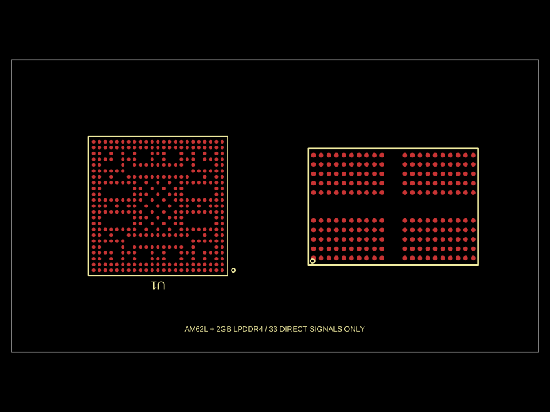 More from this author0hmX/simplified-am62l-computerThis code defines components and scripts for physically representing and routing high-speed DDR memory signals, power lines, and ground planes on an 8-layer PCB with detailed pin assignments, copper pours, and precise via and trace layouts based on TI EVM reference data.
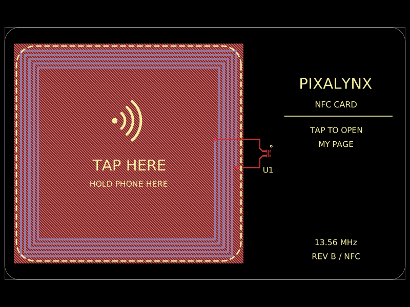 Similar packagepixalynx/pixal-nfc-cardThis code defines React components representing specific electronic hardware components—namely, a 100-ohm SMD resistor, a surface-mount LED, and a chip with labeled pins—each modeled with detailed footprints, 3D CAD models, and manufacturer part information for PCB design.
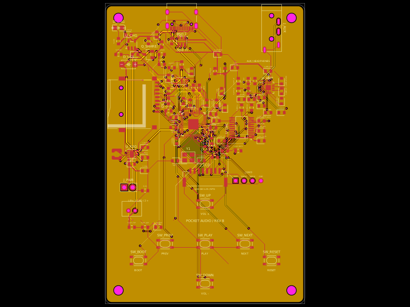 Discover something newDevesh36/pocket-audio-playerA portable, rechargeable microSD audio player built around an RP2040, SPI flash, USB‑C charging/power management, LCD/button controls, PCM5102A I²S DAC, and TPA6132A headphone amplifier in a 3D‑printed enclosure.