0hmX/arducam-mini-2mp-plus-b0067-clone
This code defines React components representing various hardware electronic components such as sensors, chips, capacitors, inductors, and memory devices, including their physical pin layouts, footprints, and 3D CAD models for PCB design integration.
- Version
- 1.0.3
- License
- unset
- Stars
- 0
index.circuit.tsx
PCB
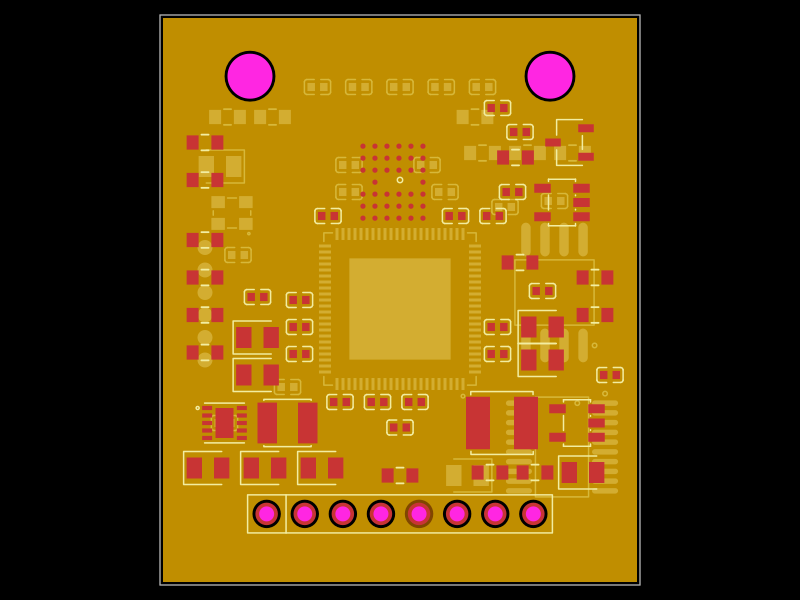
Schematic

import { AP2127K_ADJTRG1 } from "./imports/AP2127K_ADJTRG1"
import { A_0402CG150J500NT } from "./imports/A_0402CG150J500NT"
import { CL05B104KO5NNNC } from "./imports/CL05B104KO5NNNC"
import { FCC0402X105K100AT } from "./imports/FCC0402X105K100AT"
import { FNR3015S1R5MT } from "./imports/FNR3015S1R5MT"
import { GW2AR_LV18QN88C8_I7 } from "./imports/GW2AR_LV18QN88C8_I7"
import { GRM155R71C103KA01D } from "./imports/GRM155R71C103KA01D"
import { OT252027MJBA4SL } from "./imports/OT252027MJBA4SL"
import { PZ254V_11_08P } from "./imports/PZ254V_11_08P"
import { TLV62569DBVR } from "./imports/TLV62569DBVR"
import { TPS63031DSKR } from "./imports/TPS63031DSKR"
import { TXS0108EPWR } from "./imports/TXS0108EPWR"
import { W25Q64JVSSIQ } from "./imports/W25Q64JVSSIQ"
import { WPN4020H2R2MT } from "./imports/WPN4020H2R2MT"
import { XC6206P282MR } from "./imports/XC6206P282MR"
import { OV2640 } from "./components/OV2640"

export const verifiedB0067Interface = {
  connector: ["CS", "MOSI", "MISO", "SCLK", "GND", "VCC", "SDA", "SCL"],
  supply: "3.3V to 5V",
  maximumSpiClockHz: 8_000_000,
  bufferBytes: 8 * 1024 * 1024,
  sensor: "OV2640",
} as const

const c100n = [
  ["C_FPGA_VCC1", "VCC1V0", -4.0, -6.8, "top"],
  ["C_FPGA_VCC2", "VCC1V0", -1.5, -6.8, "top"],
  ["C_FPGA_VCC3", "VCC1V0", 1.0, -6.8, "top"],
  ["C_FPGA_VCC4", "VCC1V0", 0.0, -8.5, "top"],
  ["C_FPGA_IO0", "VCC3V3", -6.7, -3.6, "top"],
  ["C_FPGA_IO1", "VCC3V3", -6.7, -1.8, "top"],
  ["C_FPGA_IO3", "VCC3V3", -6.7, 0.0, "top"],
  ["C_FPGA_IO4", "VCC3V3", 6.5, -3.6, "top"],
  ["C_FPGA_IO5", "VCC3V3", 6.5, -1.8, "top"],
  ["C_FPGA_X1", "VCC3V3", -4.8, 5.6, "top"],
  ["C_FPGA_X2", "VCC3V3", 3.7, 5.6, "top"],
  ["C_FPGA_X3", "VCC3V3", 6.2, 5.6, "top"],
  ["C_FLASH", "VCC3V3", 10.3, 6.6, "bottom"],
  ["C_SENSOR_IO", "VCC3V3", 0.0, 14.2, "bottom"],
  ["C_SENSOR_AV1", "VCC2V8", -5.5, 14.2, "bottom"],
  ["C_SENSOR_AV2", "VCC2V8", -2.75, 14.2, "bottom"],
  ["C_SENSOR_DV1", "VCC1V3", 5.5, 14.2, "bottom"],
  ["C_SENSOR_DV2", "VCC1V3", 2.75, 14.2, "bottom"],
] as const

const pullResistors = [
  ["R_RECONFIG", "4.7k", "RECONFIG_N", "VCC3V3", -13.0, 4.0, "C23162", "top"],
  ["R_FASTRD", "4.7k", "FASTRD_N", "VCC3V3", -13.0, 1.5, "C23162", "top"],
  ["R_MODE0", "1k", "MODE0", "GND", -13.0, -1.0, "C21190", "top"],
  ["R_MODE1", "1k", "MODE1", "GND", -13.0, -3.5, "C21190", "top"],
  ["R_EXTR", "10k", "EXTR", "GND", 13.0, -1.0, "C25804", "top"],
  ["R_MCLK", "1k", "FLASH_CLK", "GND", 13.0, 1.5, "C21190", "top"],
  ["R_FLASH_WP", "4.7k", "FLASH_WP", "VCC3V3", 8.5, 9.8, "C23162", "bottom"],
  ["R_FLASH_HOLD", "4.7k", "FLASH_HOLD", "VCC3V3", 11.5, 9.8, "C23162", "bottom"],
  ["R_SDA", "4.7k", "CAM_SDA", "VCC3V3", -11.5, 12.2, "C23162", "bottom"],
  ["R_SCL", "4.7k", "CAM_SCL", "VCC3V3", -8.5, 12.2, "C23162", "bottom"],
  ["R_PWDN", "10k", "CAM_PWDN", "GND", 5.0, 12.2, "C25804", "bottom"],
  ["R_RESET", "4.7k", "CAM_RESET", "VCC3V3", 5.5, 9.8, "C23162", "bottom"],
  ["R_EXPST", "10k", "CAM_EXPST", "GND", -13.0, 8.0, "C25804", "top"],
  ["R_FREX", "10k", "CAM_FREX", "GND", -13.0, 10.5, "C25804", "top"],
  ["R_LEVEL_OE", "10k", "LEVEL_OE", "GND", 0.0, -11.7, "C25804", "top"],
] as const

const FerriteBead = (props: {
  name: string
  pcbX: number
  pcbY: number
  layer?: "top" | "bottom"
  connections: { pin1: string; pin2: string }
}) => (
  <chip
    {...props}
    pinLabels={{ pin1: ["1"], pin2: ["2"] }}
    manufacturerPartNumber="BLM21PG221SN1D"
    supplierPartNumbers={{ jlcpcb: ["C85840"] }}
    footprint="0805"
  />
)

export default function ArducamB0067OpenControllerClone() {
  return (
    // Engineering routing variant: the verified B0067 outline is 24.4 x
    // 34.1 mm. The wider outline provides room to move the level translator
    // away from the FPGA while preserving the verified connector locations.
    <board
      name="B0067_OPEN_CLONE"
      width="32mm"
      height="38mm"
      layers={8}
      doubleSidedAssembly
      schematicDisabled
      autorouter="default"
      pcbStyle={{ silkscreenTextVisibility: "hidden" }}
    >
      <hole pcbX={-10} pcbY={14.92} diameter="3mm" />
      <hole pcbX={10} pcbY={14.92} diameter="3mm" />

      <PZ254V_11_08P name="J1" pcbX={0} pcbY={-14.26} connections={{
        pin1: "net.HOST_CS", pin2: "net.HOST_MOSI", pin3: "net.HOST_MISO", pin4: "net.HOST_SCLK",
        pin5: "net.GND", pin6: "net.HOST_VCC", pin7: "net.HOST_SDA", pin8: "net.HOST_SCL",
      }} />

      <TXS0108EPWR name="U_LEVEL" pcbX={10.8} pcbY={-9.8} pcbRotation={90} layer="bottom" connections={{
        VCCA: "net.VCC3V3", VCCB: "net.HOST_VCC", GND: "net.GND", OE: "net.LEVEL_OE",
        A1: "net.CAM_SPI_CS", B1: "net.HOST_CS", A2: "net.CAM_SPI_MOSI", B2: "net.HOST_MOSI",
        A3: "net.CAM_SPI_MISO", B3: "net.HOST_MISO", A4: "net.CAM_SPI_SCLK", B4: "net.HOST_SCLK",
        A5: "net.CAM_SDA", B5: "net.HOST_SDA", A6: "net.CAM_SCL", B6: "net.HOST_SCL",
      }} />

      <TPS63031DSKR name="U_3V3" pcbX={-11.7} pcbY={-8.2} connections={{
        VIN: "net.HOST_VCC", VINA: "net.HOST_VCC", EN: "net.HOST_VCC", PS_SYNC: "net.GND",
        GND: "net.GND", PGND: "net.GND", EP: "net.GND", L1: "net.BB_L1", L2: "net.BB_L2",
        VOUT: "net.VCC3V3", FB: "net.VCC3V3",
      }} />
      <FNR3015S1R5MT name="L_3V3" pcbX={-7.5} pcbY={-8.2}
        connections={{ pin1: "net.BB_L1", pin2: "net.BB_L2" }} />
      <capacitor name="C_3V3_IN" capacitance="10uF" footprint="0805" manufacturerPartNumber="GRM21BR71A106KE51L"
        supplierPartNumbers={{ jlcpcb: ["C86038"] }} pcbX={-12.8} pcbY={-11.2}
        connections={{ pin1: "net.HOST_VCC", pin2: "net.GND" }} />
      <capacitor name="C_3V3_OUT1" capacitance="10uF" footprint="0805" manufacturerPartNumber="GRM21BR71A106KE51L"
        supplierPartNumbers={{ jlcpcb: ["C86038"] }} pcbX={-9.0} pcbY={-11.2}
        connections={{ pin1: "net.VCC3V3", pin2: "net.GND" }} />
      <capacitor name="C_3V3_OUT2" capacitance="10uF" footprint="0805" manufacturerPartNumber="GRM21BR71A106KE51L"
        supplierPartNumbers={{ jlcpcb: ["C86038"] }} pcbX={-5.2} pcbY={-11.2}
        connections={{ pin1: "net.VCC3V3", pin2: "net.GND" }} />
      <CL05B104KO5NNNC name="C_3V3_VINA" layer="bottom"
        pcbX={-11.7} pcbY={-8.2} connections={{ pin1: "net.HOST_VCC", pin2: "net.GND" }} />

      <TLV62569DBVR name="U_1V0" pcbX={11.8} pcbY={-8.2}
        connections={{ EN: "net.VCC3V3", GND: "net.GND", VIN: "net.VCC3V3", SW: "net.BUCK1_SW", FB: "net.BUCK1_FB" }} />
      <WPN4020H2R2MT name="L_1V0" pcbX={6.8} pcbY={-8.2}
        connections={{ pin1: "net.BUCK1_SW", pin2: "net.VCC1V0" }} />
      <resistor name="R_1V0_TOP" resistance="66.5k" footprint="0603" manufacturerPartNumber="RC0603FR-0766K5L"
        supplierPartNumbers={{ jlcpcb: ["C137691"] }} pcbX={6.0} pcbY={-11.5}
        connections={{ pin1: "net.VCC1V0", pin2: "net.BUCK1_FB" }} />
      <resistor name="R_1V0_BOT" resistance="100k" footprint="0603" supplierPartNumbers={{ jlcpcb: ["C25803"] }}
        pcbX={9.0} pcbY={-11.5} connections={{ pin1: "net.BUCK1_FB", pin2: "net.GND" }} />
      <capacitor name="C_1V0_IN" capacitance="4.7uF" footprint="0805" supplierPartNumbers={{ jlcpcb: ["C2857993"] }}
        pcbX={12.2} pcbY={-11.5} connections={{ pin1: "net.VCC3V3", pin2: "net.GND" }} />
      <capacitor name="C_1V0_OUT" capacitance="22uF" footprint="0805" layer="bottom" supplierPartNumbers={{ jlcpcb: ["C45783"] }}
        pcbX={4.5} pcbY={-11.7} connections={{ pin1: "net.VCC1V0", pin2: "net.GND" }} />

      {/* Keep the complete opposite-side projection of the FPGA package free
          of components; its decoupling rows sit outside the package bounds. */}
      <GW2AR_LV18QN88C8_I7 name="U_FPGA" pcbX={0} pcbY={-0.6} layer="bottom" connections={{
        pin1: "net.VCC1V0", pin22: "net.VCC1V0", pin45: "net.VCC1V0", pin66: "net.VCC1V0",
        pin2: "net.GND", pin21: "net.GND", pin24: "net.GND", pin43: "net.GND", pin46: "net.GND",
        pin65: "net.GND", pin68: "net.GND", pin89: "net.GND",
        pin3: "net.VCC3V3", pin12: "net.VCC3V3", pin64: "net.VCC3V3", pin23: "net.VCC3V3",
        pin44: "net.VCC3V3", pin58: "net.VCC3V3", pin67: "net.VCC3V3", pin78: "net.VCC3V3",
        pin14: "net.VCCPLL_L", pin50: "net.VCCPLL_R", pin9: "net.RECONFIG_N", pin47: "net.EXTR",
        pin57: "net.FASTRD_N", pin87: "net.MODE1", pin88: "net.MODE0", pin10: "net.CLK_27M",
        pin25: "net.CAM_D0", pin26: "net.CAM_D1", pin27: "net.CAM_D2", pin28: "net.CAM_D3",
        pin29: "net.CAM_D4", pin30: "net.CAM_D5", pin31: "net.CAM_D6", pin32: "net.CAM_D7",
        pin33: "net.CAM_VSYNC", pin34: "net.CAM_HREF", pin35: "net.CAM_PCLK", pin37: "net.CAM_XCLK",
        pin38: "net.CAM_PWDN", pin39: "net.CAM_RESET", pin69: "net.LEVEL_OE",
        pin80: "net.CAM_SPI_SCLK", pin81: "net.CAM_SPI_CS", pin82: "net.CAM_SPI_MOSI", pin83: "net.CAM_SPI_MISO",
        pin59: "net.FLASH_CLK", pin60: "net.FLASH_CS", pin61: "net.FLASH_MOSI", pin62: "net.FLASH_MISO",
        pin5: "net.JTAG_TMS", pin6: "net.JTAG_TCK", pin7: "net.JTAG_TDI", pin8: "net.JTAG_TDO",
      }} />

      <FerriteBead name="FB_PLL_L" pcbX={-9.5} pcbY={-2.5} layer="top"
        connections={{ pin1: "net.VCC1V0", pin2: "net.VCCPLL_L" }} />
      <FerriteBead name="FB_PLL_R" pcbX={9.5} pcbY={-1.8} layer="top"
        connections={{ pin1: "net.VCC1V0", pin2: "net.VCCPLL_R" }} />
      <capacitor name="C_PLL_L_4U7" capacitance="4.7uF" footprint="0805" layer="top"
        supplierPartNumbers={{ jlcpcb: ["C2857993"] }} pcbX={-9.5} pcbY={-5.0}
        connections={{ pin1: "net.VCCPLL_L", pin2: "net.GND" }} />
      <capacitor name="C_PLL_R_4U7" capacitance="4.7uF" footprint="0805" layer="top"
        supplierPartNumbers={{ jlcpcb: ["C2857993"] }} pcbX={9.5} pcbY={-4.0}
        connections={{ pin1: "net.VCCPLL_R", pin2: "net.GND" }} />
      <CL05B104KO5NNNC name="C_PLL_L_100N" layer="bottom"
        pcbX={-7.5} pcbY={-5.8} connections={{ pin1: "net.VCCPLL_L", pin2: "net.GND" }} />
      <CL05B104KO5NNNC name="C_PLL_R_100N" layer="bottom"
        pcbX={7.0} pcbY={6.2} connections={{ pin1: "net.VCCPLL_R", pin2: "net.GND" }} />
      <GRM155R71C103KA01D name="C_PLL_L_10N" layer="top"
        pcbX={-9.5} pcbY={0.2} connections={{ pin1: "net.VCCPLL_L", pin2: "net.GND" }} />
      <GRM155R71C103KA01D name="C_PLL_R_10N" layer="top"
        pcbX={9.5} pcbY={0.6} connections={{ pin1: "net.VCCPLL_R", pin2: "net.GND" }} />

      {c100n.map(([name, rail, x, y, layer]) => <CL05B104KO5NNNC key={name} name={name}
        layer={layer} pcbX={x} pcbY={y}
        connections={{ pin1: `net.${rail}`, pin2: "net.GND" }} />)}

      <OT252027MJBA4SL name="X1" pcbX={-11.2} pcbY={5.8} layer="bottom"
        connections={{ OE: "net.VCC3V3", GND: "net.GND", OUT: "net.CLK_27M", VDD: "net.OSC_VDD" }} />
      <FerriteBead name="FB_OSC" pcbX={-12.0} pcbY={8.9} layer="bottom"
        connections={{ pin1: "net.VCC3V3", pin2: "net.OSC_VDD" }} />
      <GRM155R71C103KA01D name="C_OSC" layer="bottom"
        pcbX={-10.8} pcbY={3.0} connections={{ pin1: "net.OSC_VDD", pin2: "net.GND" }} />

      <W25Q64JVSSIQ name="U_FLASH" pcbX={10.3} pcbY={0.5} layer="bottom" connections={{
        CS: "net.FLASH_CS", DO: "net.FLASH_MISO", WP: "net.FLASH_WP", GND: "net.GND",
        DI: "net.FLASH_MOSI", CLK: "net.FLASH_CLK", HOLD: "net.FLASH_HOLD", VCC: "net.VCC3V3",
      }} />

      <XC6206P282MR name="U_2V8" pcbX={11.3} pcbY={10.5} layer="top"
        connections={{ VSS: "net.GND", VOUT: "net.VCC2V8", VIN: "net.VCC3V3" }} />
      <FCC0402X105K100AT name="C_2V8_IN" layer="top"
        pcbX={8.0} pcbY={11.2} connections={{ pin1: "net.VCC3V3", pin2: "net.GND" }} />
      <FCC0402X105K100AT name="C_2V8_OUT" layer="top"
        pcbX={6.5} pcbY={12.8} connections={{ pin1: "net.VCC2V8", pin2: "net.GND" }} />

      <AP2127K_ADJTRG1 name="U_1V3" pcbX={10.8} pcbY={6.5} layer="top"
        connections={{ VIN: "net.VCC3V3", GND: "net.GND", EN: "net.VCC3V3", ADJ: "net.LDO13_ADJ", VOUT: "net.VCC1V3" }} />
      <resistor name="R_1V3_TOP" resistance="62k" footprint="0603" layer="top" supplierPartNumbers={{ jlcpcb: ["C23221"] }}
        pcbX={8.0} pcbY={2.5} connections={{ pin1: "net.VCC1V3", pin2: "net.LDO13_ADJ" }} />
      <resistor name="R_1V3_BOT" resistance="100k" footprint="0603" layer="top" supplierPartNumbers={{ jlcpcb: ["C25803"] }}
        pcbX={7.7} pcbY={9.5} connections={{ pin1: "net.LDO13_ADJ", pin2: "net.GND" }} />
      <FCC0402X105K100AT name="C_1V3_IN" layer="top"
        pcbX={14.0} pcbY={-5.0} connections={{ pin1: "net.VCC3V3", pin2: "net.GND" }} />
      <FCC0402X105K100AT name="C_1V3_OUT" layer="top"
        pcbX={7.5} pcbY={7.2} connections={{ pin1: "net.VCC1V3", pin2: "net.GND" }} />

      {/* Package and optical-array offset are verified. The optical-axis Y=8 mm
          is a documented design assumption because the legacy drawing omits it. */}
      <OV2640 name="U_SENSOR" pcbX={-0.4696} pcbY={7.855} connections={{
        DOGND: "net.GND", AGND: "net.GND", SGND: "net.GND", EGND: "net.GND", DGND1: "net.GND", DGND2: "net.GND",
        DOVDD: "net.VCC3V3", AVDD: "net.VCC2V8", SVDD1: "net.VCC2V8", SVDD2: "net.VCC2V8",
        EVDD1: "net.VCC2V8", EVDD2: "net.VCC2V8", DVDD1: "net.VCC1V3", DVDD2: "net.VCC1V3",
        VREFN: "net.CAM_VREFN", VREFH: "net.CAM_VREFH", EXPST_B: "net.CAM_EXPST", FREX: "net.CAM_FREX",
        PWDN: "net.CAM_PWDN", RESETB: "net.CAM_RESET", SIO_D: "net.CAM_SDA", SIO_C: "net.CAM_SCL",
        HREF: "net.CAM_HREF", XVCLK: "net.CAM_XCLK", VSYNC: "net.CAM_VSYNC", PCLK: "net.CAM_PCLK",
        Y2: "net.CAM_D0", Y3: "net.CAM_D1", Y4: "net.CAM_D2", Y5: "net.CAM_D3",
        Y6: "net.CAM_D4", Y7: "net.CAM_D5", Y8: "net.CAM_D6", Y9: "net.CAM_D7",
      }} />
      <CL05B104KO5NNNC name="C_VREFN" layer="bottom"
        pcbX={-3.4} pcbY={7.2} connections={{ pin1: "net.CAM_VREFN", pin2: "net.GND" }} />
      <CL05B104KO5NNNC name="C_VREFH" layer="bottom"
        pcbX={3.0} pcbY={7.2} connections={{ pin1: "net.CAM_VREFH", pin2: "net.GND" }} />
      <A_0402CG150J500NT name="C_PCLK" layer="bottom" pcbX={-3.4} pcbY={9.0}
        connections={{ pin1: "net.CAM_PCLK", pin2: "net.GND" }} />
      <CL05B104KO5NNNC name="C_RESET" layer="bottom"
        pcbX={1.8} pcbY={9.0} connections={{ pin1: "net.CAM_RESET", pin2: "net.GND" }} />

      {pullResistors.map(([name, resistance, a, b, x, y, lcsc, layer]) => <resistor key={name} name={name}
        resistance={resistance} footprint="0603" layer={layer} supplierPartNumbers={{ jlcpcb: [lcsc] }}
        pcbX={x} pcbY={y} connections={{ pin1: `net.${a}`, pin2: `net.${b}` }} />)}

      <testpoint name="TP_TMS" pcbX={-13.0} pcbY={-4.0} layer="bottom" footprintVariant="pad" padShape="circle" padDiameter="1mm" connections={{ pin1: "net.JTAG_TMS" }} />
      <testpoint name="TP_TCK" pcbX={-13.0} pcbY={-2.5} layer="bottom" footprintVariant="pad" padShape="circle" padDiameter="1mm" connections={{ pin1: "net.JTAG_TCK" }} />
      <testpoint name="TP_TDI" pcbX={-13.0} pcbY={-1.0} layer="bottom" footprintVariant="pad" padShape="circle" padDiameter="1mm" connections={{ pin1: "net.JTAG_TDI" }} />
      <testpoint name="TP_TDO" pcbX={-13.0} pcbY={0.5} layer="bottom" footprintVariant="pad" padShape="circle" padDiameter="1mm" connections={{ pin1: "net.JTAG_TDO" }} />
      <testpoint name="TP_GND" pcbX={-13.0} pcbY={2.0} layer="bottom" footprintVariant="pad" padShape="circle" padDiameter="1mm" connections={{ pin1: "net.GND" }} />
      <testpoint name="TP_3V3" pcbX={-13.0} pcbY={3.5} layer="bottom" footprintVariant="pad" padShape="circle" padDiameter="1mm" connections={{ pin1: "net.VCC3V3" }} />

      <copperpour layer="inner1" connectsTo="net.GND" unbroken clearance="0.2mm" />
      <copperpour layer="inner2" connectsTo="net.VCC3V3" unbroken clearance="0.2mm" />
    </board>
  )
}