0hmX/am3352-zcz-footprint
This code defines the physical footprint and pin layout for an 18x18 ball grid array (BGA) package of a Texas Instruments AM3352 microprocessor, including pad positions and outline drawing commands for PCB design.
- Version
- 1.0.2
- License
- unset
- Stars
- 0
README.md
# AM3352 ZCZ footprint
Reusable **footprint only** for TI AM3352BZCZ100 / ZCZ0324A (JLCPCB C468247). No board, electrical symbol, signal mapping, or 3D model is included.
## KiCad vs tscircuit verification
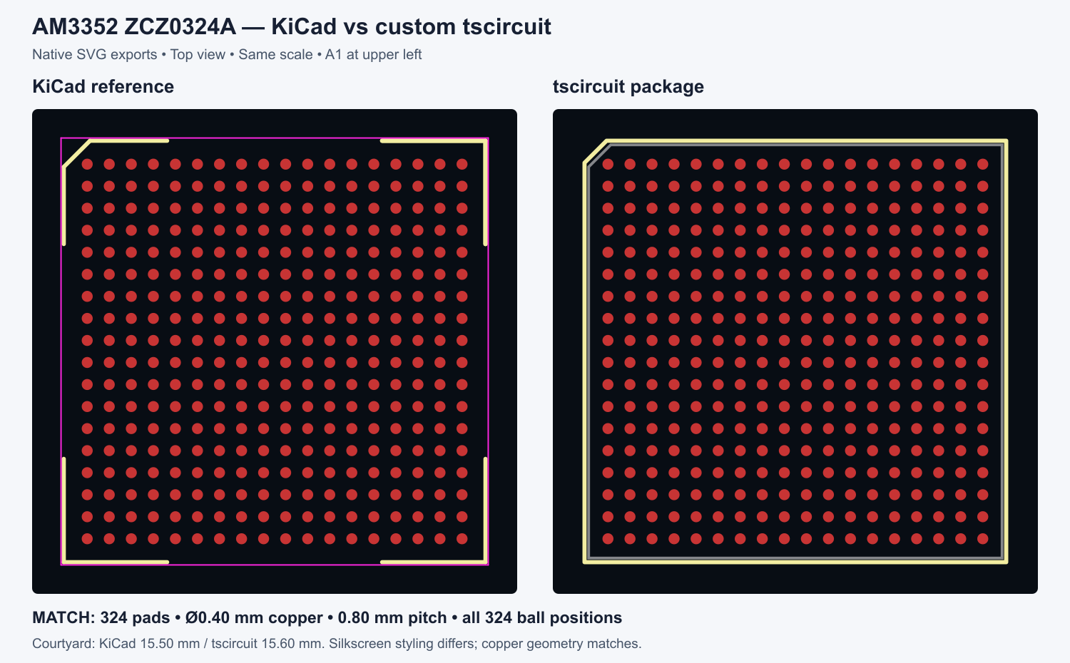
Left: native `kicad-cli fp export svg` rendering of the KiCad reference. Right: native `tsci export -f pcb-svg` rendering of this package. Both are shown from the top, at the same scale, with A1 at the upper left. Reference-designator text is hidden in the KiCad view; pad geometry is unchanged.
| Measured property | KiCad reference | This footprint |
| --- | --- | --- |
| Pad array | 18 × 18 / 324 pads | 18 × 18 / 324 pads |
| Copper pad diameter | 0.40 mm | 0.40 mm |
| Pitch | 0.80 mm | 0.80 mm |
| Outer pad-center span | 13.60 mm | 13.60 mm |
| Ball positions | Reference | All 324 match after Y-axis conversion |
| Courtyard | 15.50 × 15.50 mm | 15.60 × 15.60 mm |
The copper geometry matches. Silkscreen styling differs, and this package uses a slightly larger courtyard to allow 0.25 mm clearance beyond TI's maximum 15.1 mm body. This is a geometry comparison, not an electrical-symbol or assembly qualification. The KiCad footprint is a generic BGA reference; TI's package drawing is the design source.
## Install
```sh
tsci add 0hmX/am3352-zcz-footprint
```
## Use
```tsx
import {
AM3352ZCZFootprint,
am3352BallLabels,
} from "@tsci/0hmX.am3352-zcz-footprint"
export default () => (
<board width={22} height={22} routingDisabled>
<chip
name="U1"
pinLabels={am3352BallLabels}
footprint={<AM3352ZCZFootprint />}
/>
</board>
)
```
`AM3352ZCZFootprint` is also the default export. `am3352Balls` and the `AM3352Ball` type are available for custom symbols. Use the matching ball labels to avoid conflicting pin aliases. Numeric identifiers are column-major: pin1=A1, pin2=B1, pin19=A2. Connect by ball name, for example `U1.A1`.
## Geometry
- 324 circular pads, 18 × 18 array, 0.80 mm pitch.
- Copper diameter 0.40 mm; paste diameter 0.40 mm.
- Solder-mask expansion 0.05 mm per side.
- Body 15 × 15 mm nominal; courtyard 15.6 × 15.6 mm.
- Top view: A1 upper left, column numbers increase right, row letters increase down.
- Chamfered fabrication and silkscreen outlines identify A1.
Authored from [TI's ZCZ0324A package drawing](https://www.ti.com/lit/ds/symlink/am3352.pdf), PDF pages 260–262. All 324 pad positions and diameters were checked against the [KiCad BGA geometry reference](https://github.com/KiCad/kicad-footprints/blob/master/Package_BGA.pretty/BGA-324_15.0x15.0mm_Layout18x18_P0.8mm_Ball0.5mm_Pad0.4mm_NSMD.kicad_mod). Electrical signal assignments and manufacturing-process validation are outside this footprint package.
Related Packages
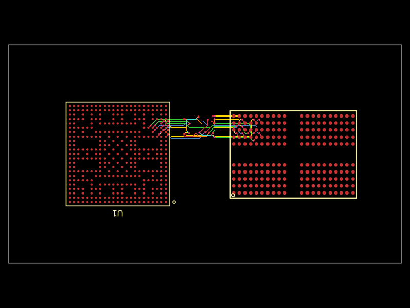 More from this author0hmX/am62l-lpddr4-breakout-reproThis code defines the physical layout, pin assignments, and power connections for the TI AM62L system-on-chip with DDR4/LPDDR4 memory, including detailed component placement, decoupling capacitors, and signal traces for a 6-layer PCB design.
 Similar packageShiboSoftwareDev/am625sip-linux-boardThis code defines the physical footprint and pin layout for an AM625 System-in-Package (SIP) component, detailing pad positions, pin labels, and package outline for hardware integration.
 Discover something newhrithik18k/smart-switch-pcbThe AO3400A component models a SOT-23 N-channel MOSFET with labeled pins for Gate, Source, and Drain, including 3D CAD models and schematic symbols for electronic circuit design.