victorev/Humax-onbard-circuit
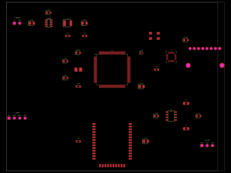
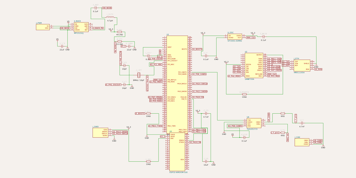
This code outlines the hardware design of an EV charger controller board featuring an ESP32 WiFi/BLE module, a W5500 Ethernet interface, a CAN transceiver for power module communication, and associated power regulation, connectors, and passive components.
- Version
- 0.0.1
- License
- unset
- Stars
- 0
index.tsx
PCB
Schematic
// EV charger supervisory controller — STM32H563 (Cortex-M33), rev B
//
// Fixes vs rev A:
//  - Inline <footprint> definitions for crystal 3225, oscillator 5032,
//    magjack RJ45, and ESP32-WROOM-32 (registry names were invalid)
//  - Board enlarged to 100x80mm; all pcbX/pcbY re-spread so nothing
//    sits inside the LQFP100 courtyard or off the board edge
//  - L_BUCK given a footprint (1210)
//
// !! Inline footprints marked PLACEHOLDER are approximate geometry.
// !! Verify pad positions against each datasheet (or swap in a verified
// !! community footprint) before generating gerbers.
// !! STM32 pin numbers still need CubeMX verification (see rev A notes).

const ESP32_PITCH = 1.27

export default () => (
  <board width="100mm" height="80mm">
    {/* ================= Power: 5V -> 3.3V buck ================= */}

    <pinheader name="J_PWR" pinCount={2} footprint="pinrow2"
      pinLabels={["V5", "GND"]} schX={-14} schY={6} pcbX={-45} pcbY={30} />

    <chip name="U_BUCK" footprint="sot23_8"
      manufacturerPartNumber="MP2315GJ"
      pinLabels={{ pin1: "EN", pin2: "VINB", pin3: "SW", pin4: "GNDB",
                   pin5: "BST", pin6: "FB", pin7: "AAM", pin8: "NCB" }}
      schX={-10} schY={6} pcbX={-30} pcbY={30} />

    <inductor name="L_BUCK" inductance="4.7uH" footprint="1210"
      schX={-7} schY={7} pcbX={-21} pcbY={30} />
    <capacitor name="C_BST" capacitance="0.1uF" footprint="0603"
      schX={-8.5} schY={8} pcbX={-30} pcbY={35} />
    <capacitor name="C_VIN" capacitance="22uF" footprint="0805"
      schX={-12} schY={4} pcbX={-38} pcbY={30} />
    <capacitor name="C_V33A" capacitance="22uF" footprint="0805"
      schX={-5} schY={4} pcbX={-13} pcbY={30} />
    <resistor name="R_FB1" resistance="40.2k" footprint="0603"
      schX={-6} schY={5.5} pcbX={-21} pcbY={24} />
    <resistor name="R_FB2" resistance="13.3k" footprint="0603"
      schX={-6} schY={4.5} pcbX={-13} pcbY={24} />

    <net name="V5" />
    <net name="V3_3" />
    <net name="GND" />
    <net name="SW_NODE" />

    <trace from=".J_PWR > .V5" to="net.V5" />
    <trace from=".J_PWR > .GND" to="net.GND" />
    <trace from=".U_BUCK > .VINB" to="net.V5" />
    <trace from=".U_BUCK > .EN" to="net.V5" />
    <trace from=".U_BUCK > .GNDB" to="net.GND" />
    <trace from=".U_BUCK > .SW" to="net.SW_NODE" />
    <trace from=".L_BUCK > .pin1" to="net.SW_NODE" />
    <trace from=".L_BUCK > .pin2" to="net.V3_3" />
    <trace from=".C_BST > .pin1" to=".U_BUCK > .BST" />
    <trace from=".C_BST > .pin2" to="net.SW_NODE" />
    <trace from=".C_VIN > .pin1" to="net.V5" />
    <trace from=".C_VIN > .pin2" to="net.GND" />
    <trace from=".C_V33A > .pin1" to="net.V3_3" />
    <trace from=".C_V33A > .pin2" to="net.GND" />
    <trace from=".R_FB1 > .pin1" to="net.V3_3" />
    <trace from=".R_FB1 > .pin2" to=".U_BUCK > .FB" />
    <trace from=".R_FB2 > .pin1" to=".U_BUCK > .FB" />
    <trace from=".R_FB2 > .pin2" to="net.GND" />

    {/* ================= STM32H563VIT6 ================= */}

    <chip name="U1" footprint="lqfp100"
      manufacturerPartNumber="STM32H563VIT6"
      pinLabels={{
        pin6:  "NRST",
        pin94: "BOOT0",
        pin11: "VDD1",
        pin10: "VSS1",
        pin12: "PH0_OSCIN",
        pin13: "PH1_OSCOUT",
        pin23: "PA1_REFCLK",
        pin24: "PA2_MDIO",
        pin15: "PC1_MDC",
        pin32: "PA7_CRSDV",
        pin33: "PC4_RXD0",
        pin34: "PC5_RXD1",
        pin47: "PB11_TXEN",
        pin51: "PB12_TXD0",
        pin52: "PB13_TXD1",
        pin81: "PD0_CANRX",
        pin82: "PD1_CANTX",
        pin68: "PA9_TX",
        pin69: "PA10_RX",
        pin72: "PA13_SWDIO",
        pin76: "PA14_SWCLK",
      }}
      schX={0} schY={0} pcbX={0} pcbY={8} />

    <trace from=".U1 > .VDD1" to="net.V3_3" />
    <trace from=".U1 > .VSS1" to="net.GND" />

    <resistor name="R_BOOT" resistance="10k" footprint="0603"
      schX={-3} schY={-3} pcbX={-16} pcbY={0} />
    <capacitor name="C_NRST" capacitance="0.1uF" footprint="0603"
      schX={-3} schY={3} pcbX={-16} pcbY={16} />
    <trace from=".R_BOOT > .pin1" to=".U1 > .BOOT0" />
    <trace from=".R_BOOT > .pin2" to="net.GND" />
    <trace from=".C_NRST > .pin1" to=".U1 > .NRST" />
    <trace from=".C_NRST > .pin2" to="net.GND" />

    {/* 8 MHz HSE crystal — PLACEHOLDER 3225 footprint, 2 pads */}
    <crystal name="X_HSE" frequency="8MHz" loadCapacitance="10pF"
      schX={-4} schY={1} pcbX={-16} pcbY={8}>
      <footprint>
        <smtpad shape="rect" width="1.4mm" height="1.9mm" pcbX={-1.1} pcbY={0} portHints={["pin1"]} />
        <smtpad shape="rect" width="1.4mm" height="1.9mm" pcbX={1.1} pcbY={0} portHints={["pin2"]} />
      </footprint>
    </crystal>
    <capacitor name="C_H1" capacitance="10pF" footprint="0603"
      schX={-5.5} schY={2} pcbX={-22} pcbY={12} />
    <capacitor name="C_H2" capacitance="10pF" footprint="0603"
      schX={-5.5} schY={0} pcbX={-22} pcbY={4} />
    <trace from=".X_HSE > .pin1" to=".U1 > .PH0_OSCIN" />
    <trace from=".X_HSE > .pin2" to=".U1 > .PH1_OSCOUT" />
    <trace from=".C_H1 > .pin1" to=".U1 > .PH0_OSCIN" />
    <trace from=".C_H1 > .pin2" to="net.GND" />
    <trace from=".C_H2 > .pin1" to=".U1 > .PH1_OSCOUT" />
    <trace from=".C_H2 > .pin2" to="net.GND" />

    <capacitor name="C_M1" capacitance="0.1uF" footprint="0402"
      schX={3} schY={3} pcbX={14} pcbY={16} />
    <capacitor name="C_M2" capacitance="4.7uF" footprint="0805"
      schX={3} schY={-3} pcbX={14} pcbY={0} />
    <trace from=".C_M1 > .pin1" to="net.V3_3" />
    <trace from=".C_M1 > .pin2" to="net.GND" />
    <trace from=".C_M2 > .pin1" to="net.V3_3" />
    <trace from=".C_M2 > .pin2" to="net.GND" />

    <pinheader name="J_SWD" pinCount={4} footprint="pinrow4"
      pinLabels={["S3V3", "SWDIO", "SWCLK", "SGND"]}
      schX={-8} schY={-5} pcbX={-45} pcbY={-15} />
    <trace from=".J_SWD > .S3V3" to="net.V3_3" />
    <trace from=".J_SWD > .SWDIO" to=".U1 > .PA13_SWDIO" />
    <trace from=".J_SWD > .SWCLK" to=".U1 > .PA14_SWCLK" />
    <trace from=".J_SWD > .SGND" to="net.GND" />

    {/* ================= LAN8720A RMII PHY ================= */}

    <chip name="U2" footprint="qfn24"
      manufacturerPartNumber="LAN8720A"
      pinLabels={{
        pin6:  "VDD2A",
        pin7:  "TXP",
        pin8:  "TXN",
        pin9:  "RXP",
        pin10: "RXN",
        pin12: "MDIO",
        pin13: "MDC",
        pin14: "REFCLKIN",
        pin16: "CRSDV",
        pin17: "RXD1",
        pin18: "RXD0",
        pin19: "VDDIO",
        pin20: "TXD1",
        pin21: "TXD0",
        pin22: "TXEN",
        pin24: "RSTPHY",
      }}
      schX={8} schY={2} pcbX={28} pcbY={14} />

    {/* 50 MHz oscillator — PLACEHOLDER 5032 footprint, 4 corner pads */}
    <chip name="U_OSC"
      manufacturerPartNumber="SIT2001-50MHz"
      pinLabels={{ pin1: "OE", pin2: "OGND", pin3: "OUT", pin4: "OVDD" }}
      schX={6} schY={5} pcbX={20} pcbY={24}>
      <footprint>
        <smtpad shape="rect" width="1.4mm" height="1.2mm" pcbX={-1.85} pcbY={-1.25} portHints={["pin1"]} />
        <smtpad shape="rect" width="1.4mm" height="1.2mm" pcbX={1.85} pcbY={-1.25} portHints={["pin2"]} />
        <smtpad shape="rect" width="1.4mm" height="1.2mm" pcbX={1.85} pcbY={1.25} portHints={["pin3"]} />
        <smtpad shape="rect" width="1.4mm" height="1.2mm" pcbX={-1.85} pcbY={1.25} portHints={["pin4"]} />
      </footprint>
    </chip>

    <net name="RMII_CLK" />
    <trace from=".U_OSC > .OVDD" to="net.V3_3" />
    <trace from=".U_OSC > .OE" to="net.V3_3" />
    <trace from=".U_OSC > .OGND" to="net.GND" />
    <trace from=".U_OSC > .OUT" to="net.RMII_CLK" />
    <trace from=".U2 > .REFCLKIN" to="net.RMII_CLK" />
    <trace from=".U1 > .PA1_REFCLK" to="net.RMII_CLK" />

    <trace from=".U2 > .VDD2A" to="net.V3_3" />
    <trace from=".U2 > .VDDIO" to="net.V3_3" />
    <trace from=".U1 > .PA2_MDIO" to=".U2 > .MDIO" />
    <trace from=".U1 > .PC1_MDC" to=".U2 > .MDC" />
    <trace from=".U1 > .PA7_CRSDV" to=".U2 > .CRSDV" />
    <trace from=".U1 > .PC4_RXD0" to=".U2 > .RXD0" />
    <trace from=".U1 > .PC5_RXD1" to=".U2 > .RXD1" />
    <trace from=".U1 > .PB11_TXEN" to=".U2 > .TXEN" />
    <trace from=".U1 > .PB12_TXD0" to=".U2 > .TXD0" />
    <trace from=".U1 > .PB13_TXD1" to=".U2 > .TXD1" />

    <resistor name="R_PHYRST" resistance="10k" footprint="0603"
      schX={7} schY={-1} pcbX={21} pcbY={8} />
    <trace from=".R_PHYRST > .pin1" to="net.V3_3" />
    <trace from=".R_PHYRST > .pin2" to=".U2 > .RSTPHY" />

    <capacitor name="C_PHY1" capacitance="0.1uF" footprint="0603"
      schX={9} schY={5} pcbX={35} pcbY={22} />
    <trace from=".C_PHY1 > .pin1" to="net.V3_3" />
    <trace from=".C_PHY1 > .pin2" to="net.GND" />

    {/* Magjack RJ45 — PLACEHOLDER: 8 signal holes + shield, verify
        against HR911105A drawing (real part has staggered rows) */}
    <chip name="J_ETH"
      manufacturerPartNumber="HR911105A"
      pinLabels={{ pin1: "TDP", pin2: "TDN", pin3: "RDP", pin6: "RDN", pin9: "SHIELD" }}
      schX={13} schY={2} pcbX={44} pcbY={14}>
      <footprint>
        <platedhole shape="circle" holeDiameter="0.9mm" outerDiameter="1.5mm" pcbX={-7.1} pcbY={4} portHints={["pin1"]} />
        <platedhole shape="circle" holeDiameter="0.9mm" outerDiameter="1.5mm" pcbX={-5.1} pcbY={4} portHints={["pin2"]} />
        <platedhole shape="circle" holeDiameter="0.9mm" outerDiameter="1.5mm" pcbX={-3.1} pcbY={4} portHints={["pin3"]} />
        <platedhole shape="circle" holeDiameter="0.9mm" outerDiameter="1.5mm" pcbX={-1.1} pcbY={4} portHints={["pin4"]} />
        <platedhole shape="circle" holeDiameter="0.9mm" outerDiameter="1.5mm" pcbX={0.9} pcbY={4} portHints={["pin5"]} />
        <platedhole shape="circle" holeDiameter="0.9mm" outerDiameter="1.5mm" pcbX={2.9} pcbY={4} portHints={["pin6"]} />
        <platedhole shape="circle" holeDiameter="0.9mm" outerDiameter="1.5mm" pcbX={4.9} pcbY={4} portHints={["pin7"]} />
        <platedhole shape="circle" holeDiameter="0.9mm" outerDiameter="1.5mm" pcbX={6.9} pcbY={4} portHints={["pin8"]} />
        <platedhole shape="circle" holeDiameter="1.6mm" outerDiameter="2.4mm" pcbX={-8} pcbY={-4} portHints={["pin9"]} />
        <platedhole shape="circle" holeDiameter="1.6mm" outerDiameter="2.4mm" pcbX={8} pcbY={-4} portHints={["pin10"]} />
      </footprint>
    </chip>
    <trace from=".U2 > .TXP" to=".J_ETH > .TDP" />
    <trace from=".U2 > .TXN" to=".J_ETH > .TDN" />
    <trace from=".U2 > .RXP" to=".J_ETH > .RDP" />
    <trace from=".U2 > .RXN" to=".J_ETH > .RDN" />
    <trace from=".J_ETH > .SHIELD" to="net.GND" />

    {/* ================= FDCAN -> power-module bus ================= */}

    <chip name="U4" footprint="soic8"
      manufacturerPartNumber="TJA1051T/3"
      pinLabels={{ pin1: "TXD", pin2: "GNDC", pin3: "VCC", pin4: "RXD",
                   pin6: "CANL", pin7: "CANH" }}
      schX={8} schY={-4} pcbX={28} pcbY={-14} />

    <trace from=".U4 > .VCC" to="net.V5" />
    <trace from=".U4 > .GNDC" to="net.GND" />
    <trace from=".U1 > .PD1_CANTX" to=".U4 > .TXD" />
    <trace from=".U4 > .RXD" to=".U1 > .PD0_CANRX" />

    <capacitor name="C_CAN" capacitance="0.1uF" footprint="0603"
      schX={7} schY={-5.5} pcbX={21} pcbY={-14} />
    <trace from=".C_CAN > .pin1" to="net.V5" />
    <trace from=".C_CAN > .pin2" to="net.GND" />

    <resistor name="R_T1" resistance="60" footprint="0805"
      schX={11} schY={-3} pcbX={35} pcbY={-8} />
    <resistor name="R_T2" resistance="60" footprint="0805"
      schX={11} schY={-5} pcbX={35} pcbY={-20} />
    <capacitor name="C_T" capacitance="4.7nF" footprint="0603"
      schX={13} schY={-4} pcbX={41} pcbY={-14} />
    <trace from=".U4 > .CANH" to=".R_T1 > .pin1" />
    <trace from=".R_T1 > .pin2" to=".C_T > .pin1" />
    <trace from=".C_T > .pin1" to=".R_T2 > .pin1" />
    <trace from=".R_T2 > .pin2" to=".U4 > .CANL" />
    <trace from=".C_T > .pin2" to="net.GND" />

    <pinheader name="J_CAN" pinCount={3} footprint="pinrow3"
      pinLabels={["CANH", "CANL", "CGND"]}
      schX={13} schY={-6} pcbX={45} pcbY={-28} />
    <trace from=".J_CAN > .CANH" to=".U4 > .CANH" />
    <trace from=".J_CAN > .CANL" to=".U4 > .CANL" />
    <trace from=".J_CAN > .CGND" to="net.GND" />

    {/* ================= ESP32 radio coprocessor ================= */}
    {/* PLACEHOLDER footprint: 38 pads generated at 1.27mm pitch
        (14 left / 10 bottom / 14 right). Verify row assignment and
        module keep-out against the ESP32-WROOM-32E datasheet. */}

    <chip name="U5"
      manufacturerPartNumber="ESP32-WROOM-32E"
      pinLabels={{ pin1: "GNDE", pin2: "VDDE", pin3: "ENE",
                   pin25: "EIO0", pin34: "ETXD0", pin35: "ERXD0" }}
      schX={0} schY={-7} pcbX={0} pcbY={-26}>
      <footprint>
        {Array.from({ length: 14 }, (_, i) => (
          <smtpad key={"l" + i} shape="rect" width="1.5mm" height="0.8mm"
            pcbX={-8.6} pcbY={8.26 - i * ESP32_PITCH}
            portHints={["pin" + (i + 1)]} />
        ))}
        {Array.from({ length: 10 }, (_, i) => (
          <smtpad key={"b" + i} shape="rect" width="0.8mm" height="1.5mm"
            pcbX={-5.715 + i * ESP32_PITCH} pcbY={-11.5}
            portHints={["pin" + (i + 15)]} />
        ))}
        {Array.from({ length: 14 }, (_, i) => (
          <smtpad key={"r" + i} shape="rect" width="1.5mm" height="0.8mm"
            pcbX={8.6} pcbY={-8.26 + i * ESP32_PITCH}
            portHints={["pin" + (i + 25)]} />
        ))}
      </footprint>
    </chip>

    <trace from=".U5 > .VDDE" to="net.V3_3" />
    <trace from=".U5 > .GNDE" to="net.GND" />
    <resistor name="R_EEN" resistance="10k" footprint="0603"
      schX={-3} schY={-8} pcbX={-16} pcbY={-26} />
    <trace from=".R_EEN > .pin1" to="net.V3_3" />
    <trace from=".R_EEN > .pin2" to=".U5 > .ENE" />

    <trace from=".U1 > .PA9_TX" to=".U5 > .ERXD0" />
    <trace from=".U5 > .ETXD0" to=".U1 > .PA10_RX" />

    <capacitor name="C_E1" capacitance="10uF" footprint="0805"
      schX={3} schY={-8} pcbX={16} pcbY={-26} />
    <trace from=".C_E1 > .pin1" to="net.V3_3" />
    <trace from=".C_E1 > .pin2" to="net.GND" />
  </board>
)