tscircuit/motor-controller
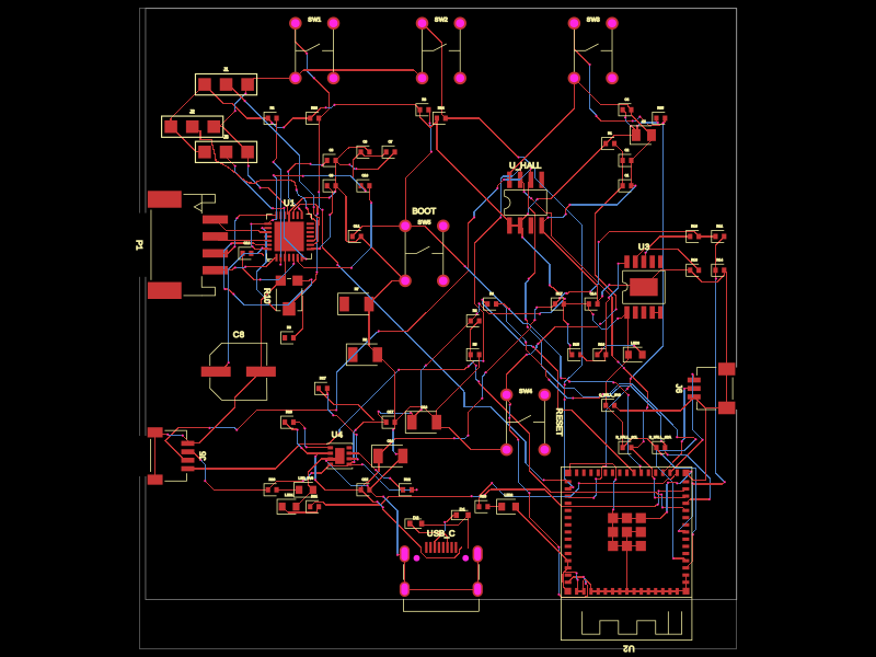
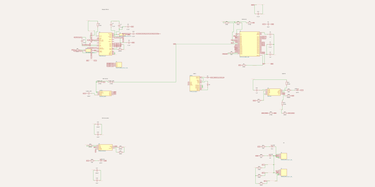
This code defines a compact hardware layout with multiple integrated components such as microcontrollers, power regulators, sensors, connectors, and passive elements, all arranged on a PCB for a versatile electronic device.
- Version
- 1.0.14
- License
- unset
- Stars
- 0
StepperDriver.tsx
PCB
Schematic
import { S4B_PH_SM4_K_TB_LF__SN_ } from "./imports/S4B_PH_SM4_K_TB_LF__SN_";
import { TMC2209_LA_T } from "./imports/TMC2209_LA_T";
import { BLA10V100M6_3_6_63TP } from "./imports/BLA10V100M6_3_6_6_3TP";
import { Potentiometer } from "imports/VGF39NCHXT_B203";

export const StepperDriver = () => (
	<group pcbX={-18} pcbY={8} schX={-18} schY={8}>
		<schematictext text="Stepper Driver" schY={7} fontSize={0.5} />

		<TMC2209_LA_T
			name="U1"
			pcbX={0}
			pcbY={0}
			schWidth={2.6}
			schPinArrangement={{
				leftSide: {
					direction: "top-to-bottom",
					pins: [
						"N_EN",
						"STEP",
						"DIR",
						"MS1_AD0",
						"MS2_AD1",
						"CLK",
						"CPI",
						"CPO",
						"SPREAD",
						"N_PD_UART",
						"VREF",
						"STDBY",
					],
				},
				rightSide: {
					direction: "top-to-bottom",
					pins: [
						"VCC_IO",
						"VS2",
						"VS1",
						"5VOUT",
						"VCP",
						"DIAG",
						"INDEX",
						"OA1",
						"OB1",
						"OA2",
						"OB2",
						"BRA",
						"BRB",
						"NC",
						"EXP",
						"GND2",
						"GND1",
					],
				},
			}}
			schPinStyle={{
				VCP: {
					marginBottom: 0.2,
				},
				DIAG: {
					marginBottom: 0.2,
				},
				INDEX: {
					marginBottom: 0.2,
				},
				OB2: {
					marginBottom: 0.2,
				},
				BRB: {
					marginBottom: 0.2,
				},
				N_EN: {
					marginBottom: 0.2,
				},
				MS2_AD1: {
					marginBottom: 0.2,
				},
				CLK: {
					marginBottom: 0.2,
				},
				CPO: {
					marginBottom: 0.2,
				},
				N_PD_UART: {
					marginBottom: 0.2,
				},
			}}
			connections={{
				EXP: "net.GND",
				GND1: "net.GND",
				GND2: "net.GND",
				VS1: "U1.VS2",
			}}
		/>

		<solderjumper
			pinCount={3}
			name="J1"
			footprint="solderjumper3"
			connections={{
				pin1: "net.VCC3",
				pin2: "U1.MS1_AD0",
				pin3: "net.GND",
			}}
			pcbX={-10}
			pcbY={18}
		/>
		<solderjumper
			pinCount={3}
			name="J2"
			footprint="solderjumper3"
			pcbX={-14}
			pcbY={13}
			connections={{
				pin1: "net.VCC3",
				pin2: "U1.MS2_AD1",
				pin3: "net.GND",
			}}
		/>
		<solderjumper
			pinCount={3}
			name="J3"
			footprint="solderjumper3"
			pcbX={-10}
			pcbY={10}
			connections={{
				pin1: "net.VCC3",
				pin2: "U1.SPREAD",
				pin3: "net.GND",
			}}
		/>
		<S4B_PH_SM4_K_TB_LF__SN_
			name="P1"
			pcbX={-12}
			pcbY={-1}
			pcbRotation={90}
			schPinArrangement={{
				leftSide: {
					direction: "top-to-bottom",
					pins: ["pin1", "pin2", "pin3", "pin4"],
				},
			}}
			connections={{
				A1: "U1.OA1",
				B1: "U1.OB1",
				A2: "U1.OA2",
				B2: "U1.OB2",
			}}
		/>

		<resistor
			name="R2"
			resistance="10k"
			footprint="0402"
			pcbX={-2}
			pcbY={14}
			connections={{
				pin1: "net.VCC3",
				pin2: "U1.N_EN",
			}}
		/>
		<resistor
			name="R6"
			resistance="100mohm"
			footprint="1206"
			pcbX={9}
			pcbY={-14}
			connections={{
				pin1: "U1.BRA",
				pin2: "net.GND",
			}}
		/>
		<resistor
			name="R7"
			resistance="100k"
			footprint="1206"
			pcbX={8}
			pcbY={-8}
			connections={{
				pin1: "U1.BRB",
				pin2: "net.GND",
			}}
		/>
		<resistor
			name="R8"
			resistance="20k"
			footprint="0402"
			supplierPartNumbers={{ jlcpcb: ["C25765"] }}
			pcbX={0}
			pcbY={-12}
			connections={{
				pin1: "net.VCC5",
				pin2: "R10.pin1",
			}}
		/>

		<Potentiometer
			symbolName="potentiometer3"
			name="R10"
			pcbX={0}
			pcbY={-7}
			pcbRotation={90}
			connections={{
				pin2: "U1.VREF",
				pin3: "net.GND",
			}}
		/>

		<capacitor
			name="C3"
			capacitance="0.1uF"
			footprint="0402"
			pcbX={5}
			pcbY={9}
			connections={{
				pin1: "U1.VCC_IO",
				pin2: "net.GND",
			}}
		/>
		<capacitor
			name="C6"
			capacitance="0.1uF"
			footprint="0402"
			pcbX={9}
			pcbY={10}
			connections={{
				pin1: "U1.VS2",
				pin2: "net.GND",
			}}
		/>
		<capacitor
			name="C7"
			capacitance="0.1uF"
			footprint="0402"
			pcbX={12}
			pcbY={10}
			connections={{
				pin1: "U1.VS2",
				pin2: "net.GND",
			}}
		/>
		<BLA10V100M6_3_6_63TP
			name="C8"
			pcbX={-6}
			pcbY={-16}
			connections={{
				pin1: "U1.VS2",
				pin2: "net.GND",
			}}
		/>
		<capacitor
			name="C9"
			capacitance="0.1uF"
			footprint="0402"
			pcbX={5}
			pcbY={6}
			connections={{
				pin1: "U1.5VOUT",
				pin2: "net.GND",
			}}
		/>
		<capacitor
			name="C10"
			capacitance="0.1uF"
			footprint="0402"
			pcbX={9}
			pcbY={6}
			connections={{
				pin1: "U1.VS2",
				pin2: "U1.VCP",
			}}
		/>
		<capacitor
			name="C12"
			capacitance="22nF"
			footprint="0402"
			pcbX={-5}
			pcbY={-2}
			connections={{
				pin1: "U1.CPI",
				pin2: "U1.CPO",
			}}
		/>
	</group>
);