techmannih/tests
Creates a 10mm x 10mm circuit board featuring an axial battery component labeled U1 at the origin.
Usage: To use this component in a project: 1. Import the component: ```tsx import { SomeComponent } from "@tsci/AUTHOR.PACKAGE_NAME" ``` 2. Place the component on a board: ```tsx <board width="20mm" height="20mm"> <SomeComponent name="U1" /> </board> ``` 3. Optionally, connect pins using `sel` from `@tscircuit/core` for tracing and connections. Key points: - Specify a unique `name` when placing the component - Use the predefined pins (VCC, DISCH, THRES, CTRL, GND, TRIG) - Customize placement with schematic/PCB coordinates if needed
- Version
- 0.0.1
- License
- unset
- Stars
- 0
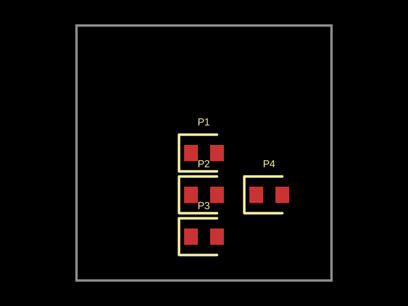
dist/pcb.svg
PCB
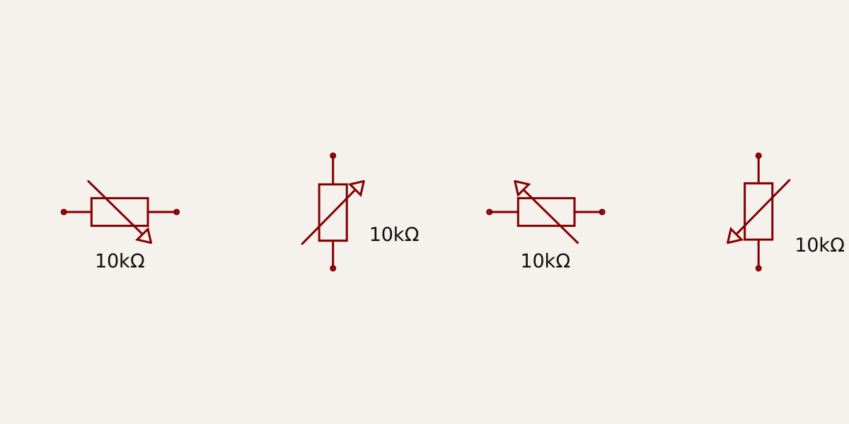
Schematic
<svg xmlns="http://www.w3.org/2000/svg" width="800" height="600" data-software-used-string="@tscircuit/core@0.0.1017"><style></style><rect class="boundary" x="0" y="0" fill="#000" width="800" height="600" data-type="pcb_background" data-pcb-layer="global"/><rect class="pcb-boundary" fill="none" stroke="#fff" stroke-width="0.3" x="150" y="50" width="500" height="500" data-type="pcb_boundary" data-pcb-layer="global"/><path class="pcb-board" d="M 150 550 L 650 550 L 650 50 L 150 50 Z" fill="none" stroke="rgba(255, 255, 255, 0.5)" stroke-width="5" data-type="pcb_board" data-pcb-layer="board"/><rect class="pcb-pad" fill="rgb(200, 52, 52)" x="361" y="284" width="27" height="32" data-type="pcb_smtpad" data-pcb-layer="top"/><rect class="pcb-pad" fill="rgb(200, 52, 52)" x="412" y="284" width="27" height="32" data-type="pcb_smtpad" data-pcb-layer="top"/><rect class="pcb-pad" fill="rgb(200, 52, 52)" x="361" y="366" width="27" height="32" data-type="pcb_smtpad" data-pcb-layer="top"/><rect class="pcb-pad" fill="rgb(200, 52, 52)" x="412" y="366" width="27" height="32" data-type="pcb_smtpad" data-pcb-layer="top"/><rect class="pcb-pad" fill="rgb(200, 52, 52)" x="361" y="448" width="27" height="32" data-type="pcb_smtpad" data-pcb-layer="top"/><rect class="pcb-pad" fill="rgb(200, 52, 52)" x="412" y="448" width="27" height="32" data-type="pcb_smtpad" data-pcb-layer="top"/><rect class="pcb-pad" fill="rgb(200, 52, 52)" x="489" y="366" width="27" height="32" data-type="pcb_smtpad" data-pcb-layer="top"/><rect class="pcb-pad" fill="rgb(200, 52, 52)" x="540" y="366" width="27" height="32" data-type="pcb_smtpad" data-pcb-layer="top"/><path class="pcb-silkscreen pcb-silkscreen-top" d="M 425.5 264 L 351 264 L 351 336 L 425.5 336" fill="none" stroke="#f2eda1" stroke-width="5" stroke-linecap="round" stroke-linejoin="round" data-pcb-component-id="pcb_component_0" data-pcb-silkscreen-path-id="pcb_silkscreen_path_0" data-type="pcb_silkscreen_path" data-pcb-layer="top"/><text x="0" y="0" dx="0" dy="0" fill="#f2eda1" font-family="Arial, sans-serif" font-size="20" text-anchor="middle" dominant-baseline="central" transform="matrix(1,0,0,1,400,239)" class="pcb-silkscreen-text pcb-silkscreen-top" data-pcb-silkscreen-text-id="pcb_component_0" stroke="none" data-type="pcb_silkscreen_text" data-pcb-layer="top">P1</text><path class="pcb-silkscreen pcb-silkscreen-top" d="M 425.5 346 L 351 346 L 351 418 L 425.5 418" fill="none" stroke="#f2eda1" stroke-width="5" stroke-linecap="round" stroke-linejoin="round" data-pcb-component-id="pcb_component_1" data-pcb-silkscreen-path-id="pcb_silkscreen_path_1" data-type="pcb_silkscreen_path" data-pcb-layer="top"/><text x="0" y="0" dx="0" dy="0" fill="#f2eda1" font-family="Arial, sans-serif" font-size="20" text-anchor="middle" dominant-baseline="central" transform="matrix(1,0,0,1,400,321)" class="pcb-silkscreen-text pcb-silkscreen-top" data-pcb-silkscreen-text-id="pcb_component_1" stroke="none" data-type="pcb_silkscreen_text" data-pcb-layer="top">P2</text><path class="pcb-silkscreen pcb-silkscreen-top" d="M 425.5 428 L 351 428 L 351 500.00000000000006 L 425.5 500.00000000000006" fill="none" stroke="#f2eda1" stroke-width="5" stroke-linecap="round" stroke-linejoin="round" data-pcb-component-id="pcb_component_2" data-pcb-silkscreen-path-id="pcb_silkscreen_path_2" data-type="pcb_silkscreen_path" data-pcb-layer="top"/><text x="0" y="0" dx="0" dy="0" fill="#f2eda1" font-family="Arial, sans-serif" font-size="20" text-anchor="middle" dominant-baseline="central" transform="matrix(1,0,0,1,400,403)" class="pcb-silkscreen-text pcb-silkscreen-top" data-pcb-silkscreen-text-id="pcb_component_2" stroke="none" data-type="pcb_silkscreen_text" data-pcb-layer="top">P3</text><path class="pcb-silkscreen pcb-silkscreen-top" d="M 553.5 346 L 479 346 L 479 418 L 553.5 418" fill="none" stroke="#f2eda1" stroke-width="5" stroke-linecap="round" stroke-linejoin="round" data-pcb-component-id="pcb_component_3" data-pcb-silkscreen-path-id="pcb_silkscreen_path_3" data-type="pcb_silkscreen_path" data-pcb-layer="top"/><text x="0" y="0" dx="0" dy="0" fill="#f2eda1" font-family="Arial, sans-serif" font-size="20" text-anchor="middle" dominant-baseline="central" transform="matrix(1,0,0,1,528,321)" class="pcb-silkscreen-text pcb-silkscreen-top" data-pcb-silkscreen-text-id="pcb_component_3" stroke="none" data-type="pcb_silkscreen_text" data-pcb-layer="top">P4</text></svg>