techmannih/nema34-mounted-stepper-controller
A 48 V USB‑C PD 3.1 EPR NEMA‑34 stepper controller PCB combining STM32/TMC5160 control, external MOSFET motor bridges, protected power and regenerative braking, USB data, telemetry, diagnostics, status LEDs, and buzzer alarms.
- Version
- 0.3.92
- License
- unset
- Stars
- 1
scripts/clean-silkscreen.py
#!/usr/bin/env python3
"""Maintain silk geometry without hiding references or changing copper."""

from __future__ import annotations

import argparse
import math
import re
from pathlib import Path

import pcbnew
import wx


def clip_passive_outlines(board, footprints):
    """Trim passive outline strokes where solder lands or other markings occupy the ink area."""
    obstacles = []
    candidates = []
    held = []

    def remember(reference, item, layer=None):
        shape = item.GetEffectiveShape(layer) if layer is not None else item.GetEffectiveShape()
        obstacles.append((reference, item.GetBoundingBox(), shape))

    for footprint in footprints:
        reference = footprint.GetReference()
        for pad in footprint.Pads():
            held.append(pad)
            if pad.IsOnLayer(pcbnew.F_Cu):
                remember(None, pad, pcbnew.F_Cu)
        for graphic in footprint.GraphicalItems():
            held.append(graphic)
            if graphic.GetLayer() != pcbnew.F_SilkS:
                continue
            if (re.fullmatch(r"[RC]\d+", reference)
                    and isinstance(graphic, pcbnew.PCB_SHAPE)
                    and graphic.GetShape() == pcbnew.SHAPE_T_SEGMENT):
                candidates.append((footprint, graphic))
            else:
                remember(reference, graphic)
    for drawing in board.GetDrawings():
        held.append(drawing)
        if drawing.GetLayer() == pcbnew.F_SilkS:
            remember(None, drawing)

    clipped = []
    for footprint, graphic in sorted(candidates, key=lambda pair: (pair[0].GetReference(), pair[1].GetStart().x, pair[1].GetStart().y)):
        start, end = graphic.GetStart(), graphic.GetEnd()
        length = math.hypot(end.x - start.x, end.y - start.y)
        steps = max(1, math.ceil(length / pcbnew.FromMM(0.01)))
        radius = int(graphic.GetWidth() / 2 + pcbnew.FromMM(0.12))
        bounds = graphic.GetBoundingBox()
        bounds.Inflate(radius)
        nearby = [shape for reference, box, shape in obstacles
                  if reference != footprint.GetReference() and bounds.Intersects(box)]

        def position(index):
            return pcbnew.VECTOR2I(round(start.x + (end.x - start.x) * index / steps),
                                 round(start.y + (end.y - start.y) * index / steps))

        # A 10 um sampling interval and 120 um clearance leave a margin over
        # the 100 um silkscreen rule; the result still requires native DRC.
        clear = [not any(shape.Collide(position(index), radius) for shape in nearby)
                 for index in range(steps + 1)]
        if all(clear):
            remember(footprint.GetReference(), graphic)
            continue
        runs, first = [], None
        for index, available in enumerate(clear + [False]):
            if available and first is None:
                first = index
            if not available and first is not None:
                if (index - 1 - first) * length / steps >= pcbnew.FromMM(0.2):
                    runs.append((first, index - 1))
                first = None
        footprint.Remove(graphic)
        for first, last in runs:
            segment = pcbnew.PCB_SHAPE(footprint)
            segment.SetShape(pcbnew.SHAPE_T_SEGMENT)
            segment.SetLayer(pcbnew.F_SilkS)
            segment.SetWidth(graphic.GetWidth())
            segment.SetStart(position(first))
            segment.SetEnd(position(last))
            footprint.Add(segment)
            held.append(segment)
            remember(footprint.GetReference(), segment)
        clipped.append({"reference": footprint.GetReference(), "retained_segments": len(runs)})
    # Keep SWIG-owned shape and item wrappers alive through SaveBoard.
    return clipped, (held, obstacles, candidates)


def main() -> None:
    parser = argparse.ArgumentParser()
    parser.add_argument("board", type=Path)
    parser.add_argument("--clip-passive-outlines", action="store_true",
                        help="Trim only R/C outline strokes that collide with solder lands or adjacent markings")
    args = parser.parse_args()

    app = wx.App(False)
    board = pcbnew.LoadBoard(str(args.board))
    footprints = list(board.GetFootprints())
    clipped, clipping_objects = clip_passive_outlines(board, footprints) if args.clip_passive_outlines else ([], None)
    settings = board.GetDesignSettings()
    settings.m_AllowSoldermaskBridgesInFPs = True
    settings.m_TrackMinWidth = pcbnew.FromMM(0.09)
    settings.m_ViasMinSize = pcbnew.FromMM(0.50)
    settings.m_MinThroughDrill = pcbnew.FromMM(0.30)
    settings.m_CopperEdgeClearance = pcbnew.FromMM(0.20)
    # USB4105's manufacturer footprint has 0.145 mm between the locating
    # NPTH and adjacent copper.  The value below covers that fixed geometry;
    # ordinary routing still follows the 0.09 mm trace/space and 0.20 mm edge
    # rules recorded in board-standards.json.
    settings.m_HoleClearance = pcbnew.FromMM(0.13)
    settings.m_MinSilkTextHeight = pcbnew.FromMM(0.80)
    netclass = settings.m_NetSettings.GetDefaultNetclass()
    netclass.SetClearance(pcbnew.FromMM(0.09))
    netclass.SetTrackWidth(pcbnew.FromMM(0.15))
    netclass.SetViaDiameter(pcbnew.FromMM(0.50))
    netclass.SetViaDrill(pcbnew.FromMM(0.30))
    removed = []
    updated = []
    resized = []
    embedded_footprints = 0
    for footprint in footprints:
        fpid = footprint.GetFPID()
        # tscircuit exports fully embedded custom footprints, not references to
        # an installed external library.  Clear the stale library nickname so
        # KiCad validates the embedded geometry itself.
        if fpid.GetLibNickname():
            footprint.SetFPID(pcbnew.LIB_ID("", fpid.GetLibItemName()))
            embedded_footprints += 1
        for field in footprint.GetFields():
            # Keep the footprint's native reference size and position.
            if field.GetText() == footprint.GetReference():
                continue
            if pcbnew.ToMM(field.GetTextHeight()) < 0.8:
                field.SetTextHeight(pcbnew.FromMM(0.8))
                resized.append(field.GetText())
    for drawing in list(board.GetDrawings()):
        if not isinstance(drawing, pcbnew.PCB_TEXT) or drawing.GetLayer() not in (pcbnew.F_SilkS, pcbnew.B_SilkS):
            continue
        text = drawing.GetText().strip()
        if drawing.GetLayer() == pcbnew.F_SilkS and text.startswith("PD1180-EPR"):
            drawing.SetText("PD1180-EPR — NEMA 34 Smart Motor-Mounted")
            updated.append(text)
        elif drawing.GetLayer() == pcbnew.F_SilkS and text == "48V EPR CONTROLLER":
            drawing.SetText("Stepper Controller with USB-C PD 3.1 EPR · r0.4 ECO")
            updated.append(text)
        if pcbnew.ToMM(drawing.GetTextHeight()) < 0.8:
            drawing.SetTextHeight(pcbnew.FromMM(0.8))
            resized.append(text)
    pcbnew.SaveBoard(str(args.board), board)
    print({
        "passive_references_removed": len(removed),
        "version_labels_updated": len(updated),
        "silkscreen_text_resized": len(resized),
        "same_footprint_mask_bridges_allowed": True,
        "embedded_footprint_ids_normalized": embedded_footprints,
        "minimum_trace_space_mm": 0.09,
        "usb_connector_npth_clearance_mm": 0.13,
        "clipped_passive_outline_segments": clipped,
    })


if __name__ == "__main__":
    main()
Related Packages
 More from this authortechmannih/schematic-testA PCB with a 6-pin SPI display connector linked to SPI signals, ground, and 3.3V power.
 Similar packageimrishabh18/rp2040-motor-controllerAn RP2040-based NEMA17 stepper-motor controller with USB-C programming and PD motor-power negotiation, DRV8825 dual H-bridge drive, current/temperature telemetry, protected power filtering, status RGB LED, buzzer alarm, and optional magnetic encoder.
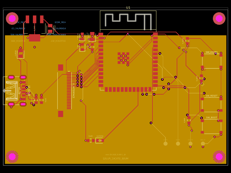 Discover something newShiboSoftwareDev/muse-m5stack-stickc-plus2-replacementA 4-layer ESP32-S3 carrier board with USB-C 5V input, AMS1117 3.3V regulation, buttons, status LED, decoupling passives, and a 24-pin FFC interface for display, touch, audio, or sensor peripherals.